IPC 7711A.pdf - 第232页
NOTE The bonding tip should be as small as possible but should completely cover the entire surface of the conductor. 7. After the bonding cycle lift the bonding tool and remove the tape used for align- ment. The film is …
OUTLINE
This method is used to re-bond a lifted conductor. Dry film epoxy is used to re-bond
the lifted conductor.
CAUTION
This method should not be used to re-bond a conductor that has been stretched or
damaged
REFERENCES
2.1 Handling Electronic Assemblies
2.2 Cleaning
2.5 Baking and Preheating
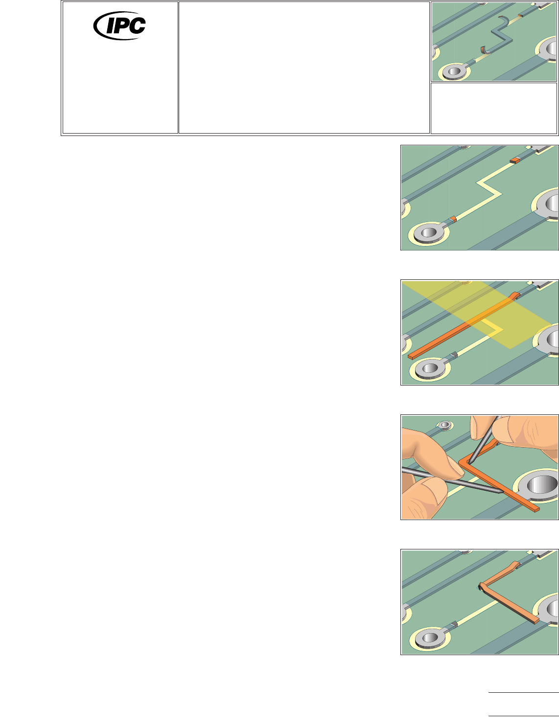
TOOLS & MATERIALS
Bonding Iron
Bonding System
Bonding Tips
Cleaner
Cleaner Wipes
Dry Film Epoxy
Polyimide Tape
Knife
Microscope
Scraper
Tweezers
PROCEDURE
1. Clean the area.
2. Remove any obstructions that prevent the lifted conductor from making contact
with the base board surface.
CAUTION
Be careful while cleaning and removing all obstructions, not to stretch or dam-
age the lifted conductor.
3. Clean the area.
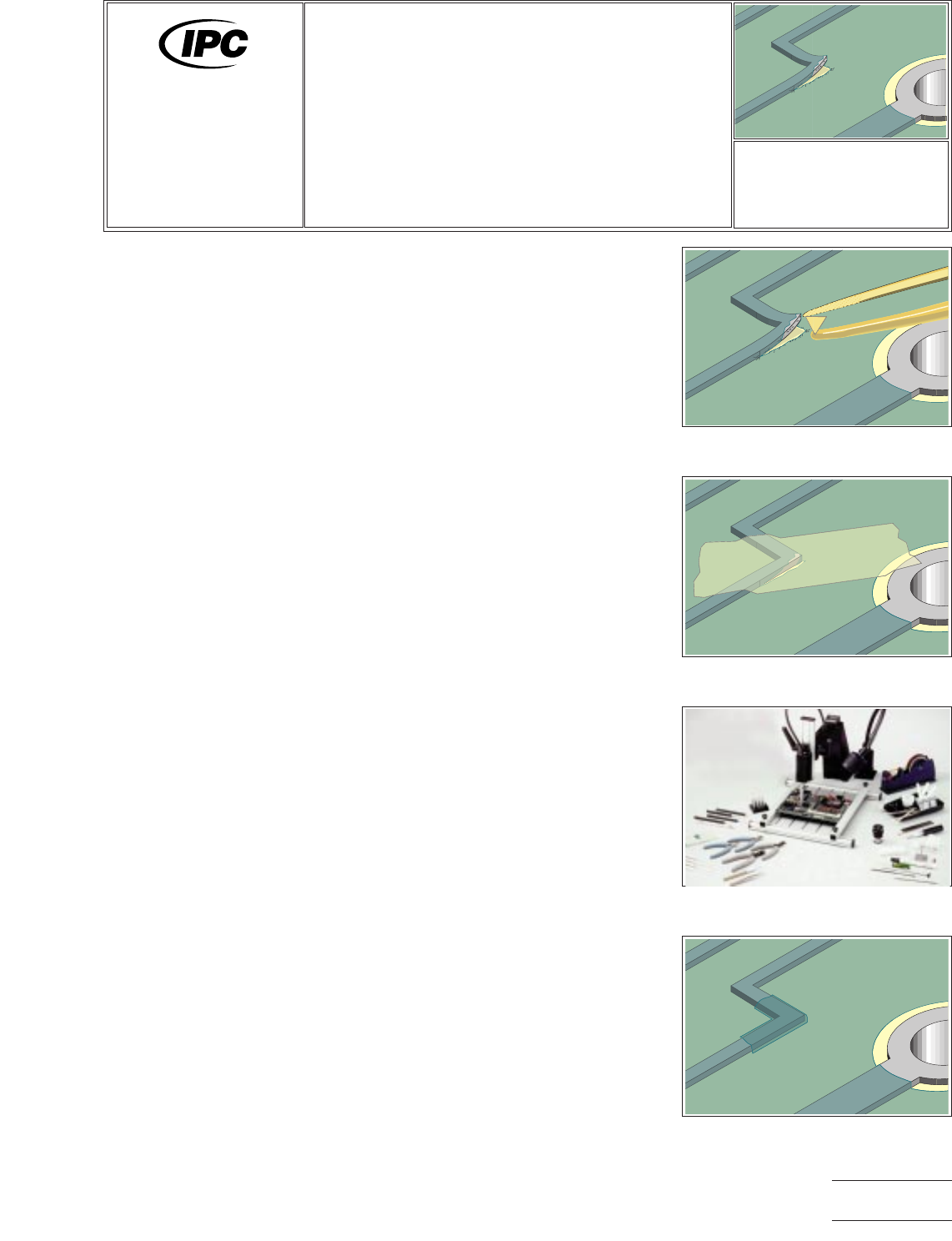
4. Cut out a piece of dry film epoxy that closely matches the size of the lifted con-
ductor. Be careful not to contaminate the dry film epoxy with materials that
could reduce the bond strength. (See Figure 1.)
NOTE
Dry film epoxy thickness should be selected to meet the requirements of the
printed wiring board.
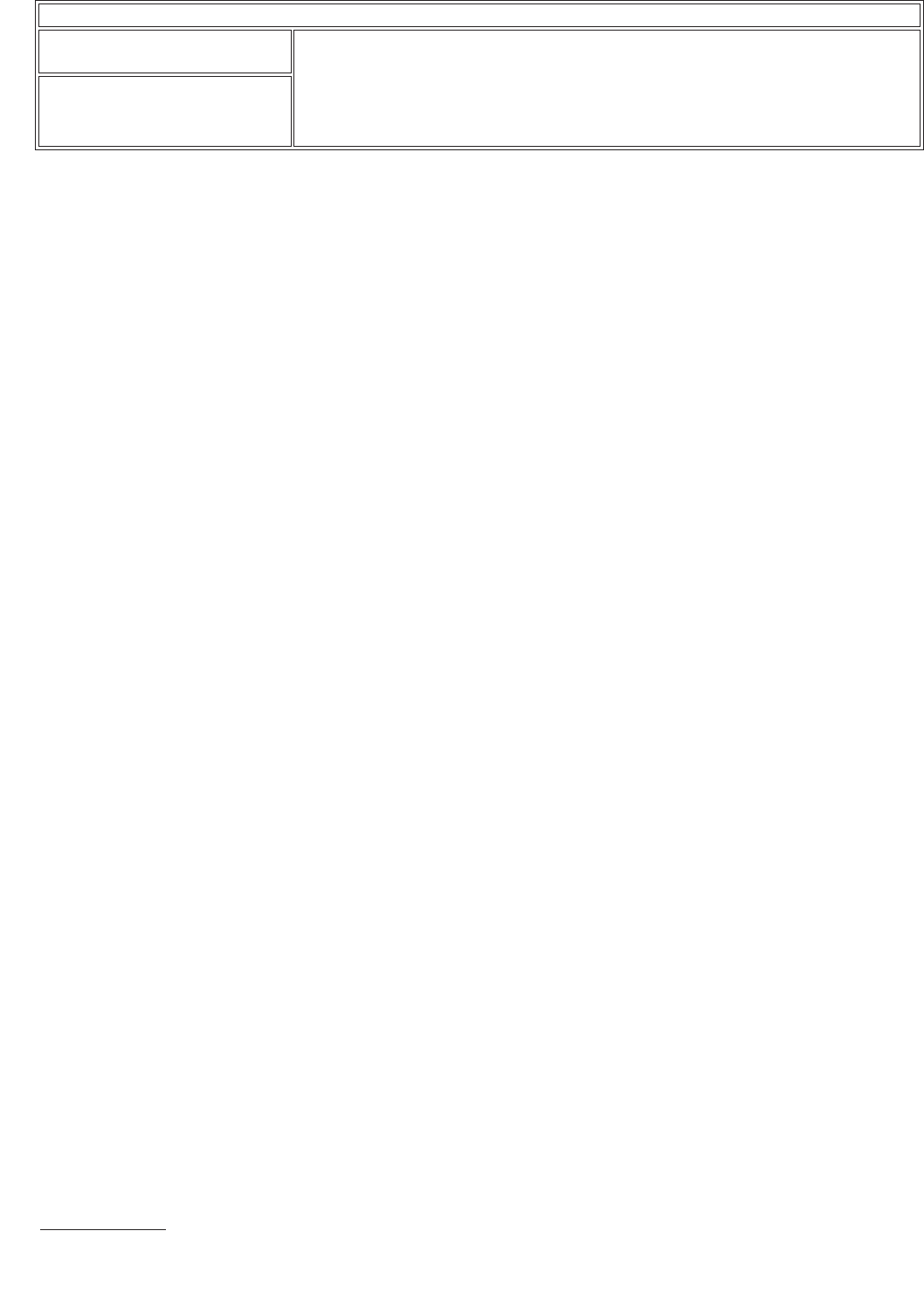
5. Place a piece of Polyimide tape over the lifted conductor. Leave the tape in
place during the bonding cycle. (See Figure 2.)
6. Position the printed wiring board so that it is flat and stable. Gently place the hot
bonding tip onto the tape covering the conductor. Apply pressure and heat per
equipment manufacturer’s recommendation. (See Figure 3.)
Figure 1 Place a piece of dry film
epoxy under lifted conductor.
Figure 2 Place tape over the lifted
conductor.
Figure 3 Bond the lifted conductor
using a bonding system.
Figure 4 Completed repair.
7721A
Repair and
Modification of
Printed Boards and
Electronic Assemblies
Revision:
Date: 2/98
Lifted Conductor Repair,
Film Adhesive Method
Number: 4.1.2
Product Class: R, F
Skill Level: Intermediate
Level of Conformance: High
Material in this manual was voluntarily established by Technical Committees of IPC. This material is advisory only and its use
or adaptation is entirely voluntary. IPC disclaims all liability of any kind as to the use, application, or adaptation of this material.
Users are also wholly responsible for protecting themselves against all claims or liabilities for patent infringement. Equipment
referenced is for the convenience of the user and does not imply endorsement by IPC.
Page1of2
Copyright Association Connecting Electronics Industries
Provided by IHS under license with IPC
Not for Resale
No reproduction or networking permitted without license from IHS
--``,``,-`-`,,`,,`,`,,`---
NOTE
The bonding tip should be as small as possible but should completely cover the
entire surface of the conductor.
7. After the bonding cycle lift the bonding tool and remove the tape used for align-
ment. The film is fully cured. Carefully clean the area and inspect the conductor.
8. Replace surface coating to match prior coating as required.
EVALUATION
1. Visual examination and tape test per IPC-TM-650, Test Method 2.4.1.
2. Electrical tests as applicable.
NOTES
IPC-7721A
Number: 4.1.2
Revision:
Date: 2/98
Subject: Lifted Conductor Repair, Film Adhesive Method
Page2of2
Copyright Association Connecting Electronics Industries
Provided by IHS under license with IPC
Not for Resale
No reproduction or networking permitted without license from IHS
--``,``,-`-`,,`,,`,`,,`---
OUTLINE
This method is used on printed wiring boards to replace damaged or missing con-
ductors on the printed wiring board surface.
CAUTION
The conductor widths, spacing and current carrying capacity must not be reduced
below allowable tolerances.
REFERENCES
2.1 Handling Electronic Assemblies
2.2 Cleaning
2.5 Baking and Preheating
2.6 Epoxy Mixing and Handling
TOOLS AND MATERIALS
Buffer
Cleaner
Conductor Foil Jumpers
Color Agent
Various Colors
Epoxy
Hand Held Drill
Heat Lamp
Polyimide Tape
Knife
Light
Liquid Flux
Microscope
Oven
Scraper
Solder
Solder Iron
with Tips
Wipes
PROCEDURE
1. Clean the area.
2 Remove the damaged section of conductor using a knife. The damaged con-
ductor should be trimmed back to a point where the conductor still has a good
bond to the printed wiring board surface.
NOTE
Heat can be applied to the damaged conductor using a soldering iron to allow
the conductor to be removed more easily.
3. Use a knife and scrape off any solder resist or coating from the ends of the
remaining conductor. (See Figure 1.)
4. Remove all loose material. Clean the area.
NOTE
It is essential that the board surface be smooth and flat. If the base material is
damaged see appropriate procedure.
Figure 1 Scrape off any coating from
the ends of the remaining conductors.
Figure 2
Place the new foil jumper in
position, hold in place with tape conductor.
Figure 3 Bend foil jumper using 2
wood sticks.
Figure 4 Wide conductors may be
folded over.
7721A
Repair and
Modification of
Printed Boards and
Electronic Assemblies
Revision: A
Date: 11/99
Conductor Repair, Foil
Jumper, Epoxy Method
Number: 4.2.1
Product Class: R, F, C
Skill Level: Advanced
Level of Conformance: Medium
Material in this manual was voluntarily established by Technical Committees of IPC. This material is advisory only and its use
or adaptation is entirely voluntary. IPC disclaims all liability of any kind as to the use, application, or adaptation of this material.
Users are also wholly responsible for protecting themselves against all claims or liabilities for patent infringement. Equipment
referenced is for the convenience of the user and does not imply endorsement by IPC.
Page1of4
Copyright Association Connecting Electronics Industries
Provided by IHS under license with IPC
Not for Resale
No reproduction or networking permitted without license from IHS
--``,``,-`-`,,`,,`,`,,`---