YesAX V3.1.2 - Software User Manual.pdf - 第112页
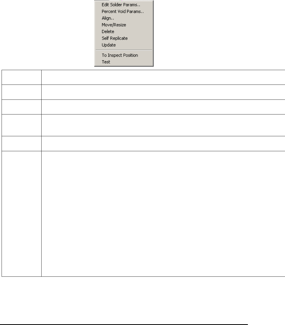
10 - 18 General Inspecti on Methodolo gy After the solder inspection box is created, you can display the solder pop-up menu by pressing the right mouse button while pointing inside the solder inspec tion box. Edit Solder…
General Inspection Methodology 10-17
The Pad Size field specifies the size of inspection area used to detect bond attach joints. If it is
set to 25%, it means that software will look for the bond attach inside 25% of the total lead
inspection box. Inside the result screen the detected bond attach locations are circled in green.
The two horizontal green lines together with the lead box on top and bottom indicate the
inspection area for bond attach. These are also called pad areas.
The bond wire in between two attached joints is supposedly to be brighter than joints but darker
than the background. To detect the bond wire session close to the bond attach joint, the
difference of gray levels between bond wire and bond attach can be used as a reference to setup
the Threshold Delta parameter values. Since top session and bottom session can have different
background, the Threshold Delta for top and bottom session can be set separated.
The green line which connects two detected bond section inside the result diagram indicates the
ideal bond locations. In reality the bond wires are not always as straight. The actual bond wire
location and the ideal green line form the exit angle for current wire bond. A large exit angle
could indicate a defect. If either the top or bottom exit angle is greater than the number specified
in Exit Angle Deviation filed, the bond wire inspection will fail. If the bond wire is missing
around the bond joint or cannot be detected, the exit angle will be set to 0 and the inspection will
fail. Sometimes the background of bond attach joint is really dark and it is hard to distinguish the
bond wire from the background. To avoid any false calls the Threshold Delta parameter can be
set to 0 so software will not calculate the exit angle and no failure regarding the exit angle will
be reported.
Other than detecting bond wire sessions around bond joints, the Wire Bond inspection will also
look for bond wire sessions inside the inspection box, within a pre-defined area. The dimension
and location of this area can be set up via the Mid Span Box X, Y and Mid Span Box Size X, Y
fields inside the Bond Wire Parameters dialog box. The yellow box shown in result dialog
represents this mid span box. To better separate bond wire from the background, the Wire
Threshold can be setup by moving the slider bar underneath. Once the bond wire has been
detected inside the mid span box, the orientation and location of the bond wire will be compared
with the green line which indicates the ideal location. The displacement and angle deviation will
be calculated and compared with the threshold values set up in Displacement Tolerance and Mid
Span Angle Tolerance fields.
10.4 Solder Inspection
Solder inspection is designed to verify the solder quality on each individual pin of the component.
The default inspection uses histogram analysis to detect insufficient solder conditions.
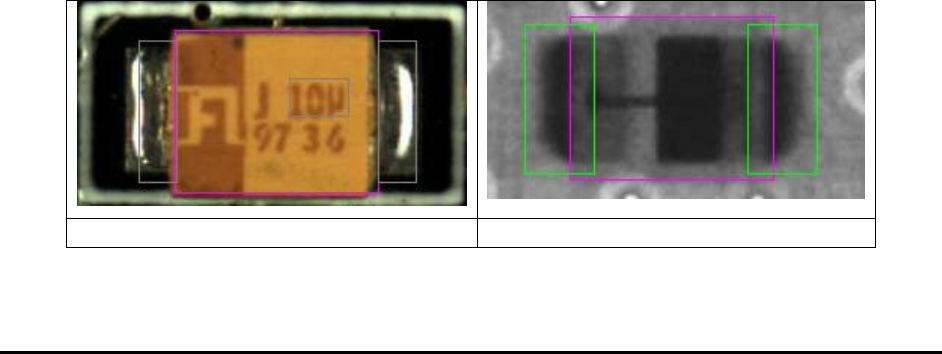
Side light Top Camera Image
Same Part Top X-ray Image
10-18 General Inspection Methodology
After the solder inspection box is created, you can display the solder pop-up menu by
pressing the right mouse button while pointing inside the solder inspection box.
Edit Solder
Params..
Launches the Solder Parameters dialog. See 10.4.1 Edit Solder Parameters.
Histogram
Setup
Launches the Histogram Parameters dialog. See 10.4.2 Histogram Parameters.
Pat Match
Param..
Launches the Pattern Matching Parameter dialog. See 10.4.3 Pattern Matching Parameters.
X-ray
Solder
Setup
Launches the X-ray Solder Parameters dialog. See 10.4.4 X-Ray Solder Parameters.
Solder Blob
Params
Launches the Solder Blob Analysis Parameters dialog. See 10.4.5 Solder Blob Analysis
Parameters.
Align..
Launches the Solder Alignment dialog for the user to align the solder inspection boxes. See
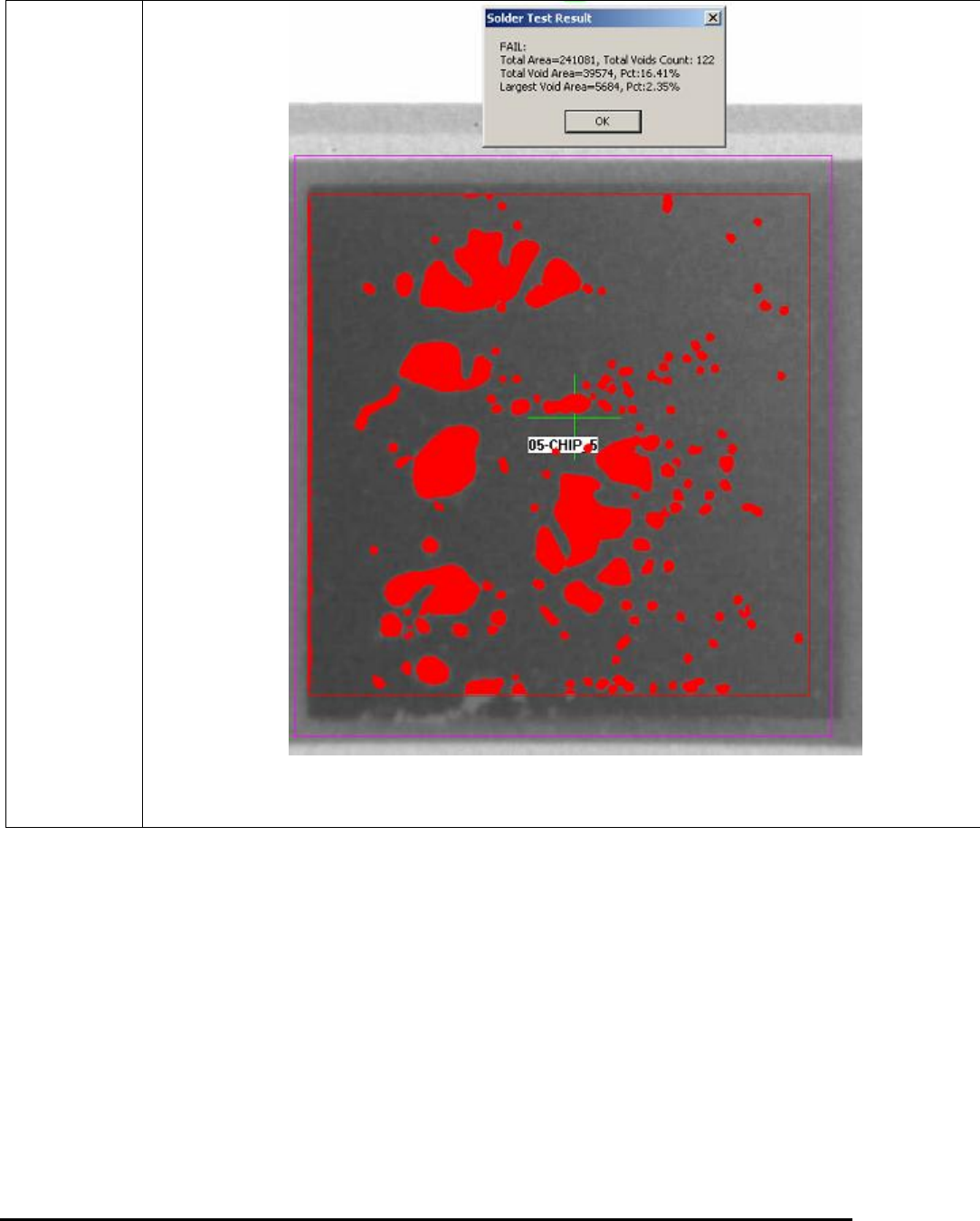
10.4.6 Percent Void Parameters
The Percent Void inspection enables measurement of the number of pixels and the percentage of
pixels in a user selected window within a defined gray scale range. The Percent Void function is
designed primarily for semiconductor applications such as measuring an area of a device which
may show some bonding inconsistencies, bonding voids, solder voids, air gaps and provide the
user with a percentage of the area that may be affected. The percent void measurement can be
applied to many other measurements where an area defect or point of interest is concerned.
The function computes the total number of pixels, the number of highlighted, “lit”, pixels and the
number of pixels in the largest lit blob within the windowed area. It determines the percentage of
lit pixels and the percentage of pixels in the largest lit blob, and then compares them with the
pass/fail thresholds set in the Max Void and the Largest Void fields. If either percentage is more
than its threshold, the system reports that Percent Void failed; otherwise, it is reported to have
passed.
The Percent Void result is presented in the Solder Test Result dialog box as shown below. By
default the void area been detected will be shown in red.
General Inspection Methodology 10-19
Select Percent Void Params from the Solder pop-up menu to open the Percent Void Parameters
dialog.