JUKI KE775点胶机说明书1.pdf - 第18页
CHAPTER1GENERAL 1ˉ 1ˉ 7.Printed circu∶ t board specifications ■ BOard sIze ■ BOard thickness ■ BOard warp ■ Board Ⅱ mⅡ a刂 ons ⊥ 3mm T Min.board size∶ X50mmXY30mm Note1 MaX,board size∶ X410mmXY360mm Note2 X∶ Along the mov…
CHAPTER1GENERAL
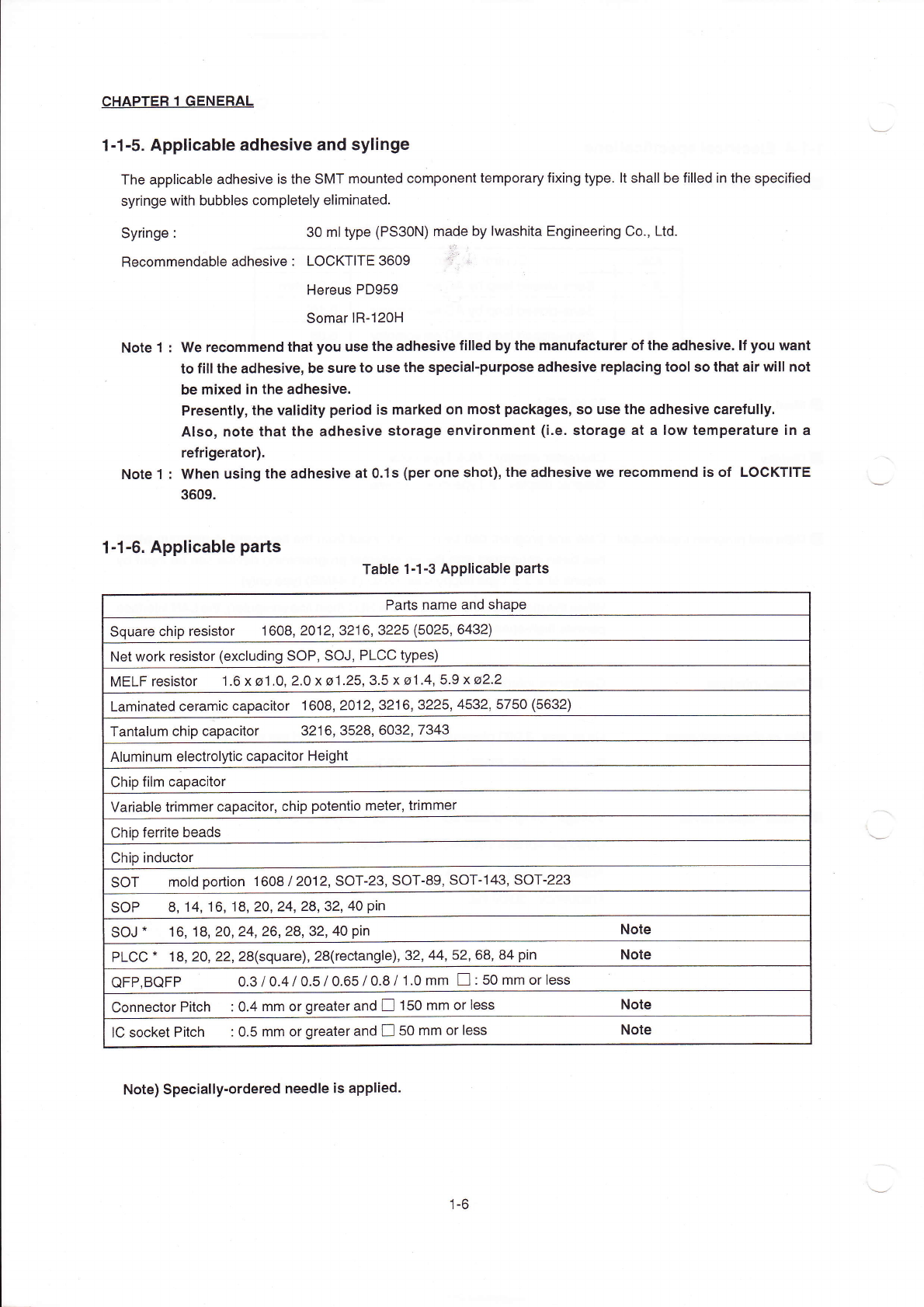
1ˉ 1ˉ5。
AppⅡ cable adhesive and syⅡ
nge
The appⅡ
cable adhesiVe is the SMT mounted componenttemporary fixing type."sha"be f"led in the spec亻
ied
syringe vv"h bubbIes Completely eⅡ
minated.
Sy"nge∶
30mltype(PS30N)rna-e bylwash"a EngineeⅡ
ng Co,Ltd.
Recommendable adhesive∶
L0CKTITE3609
∵
∷
∵
Hereus PD959
somarlRˉ
120H
Note1: We re0oⅡ
lmend that you use the adhesive f:I】
ed bythe:nanufacturer ofthe adhesive.If you want
to fi"the adhesive,be sure to use the specia卜
purpose adhesive repIacing tooI so that a∶
r Ψv∶ Ⅱ not
be:n:xed in the adhesiˇ
e.
PresentIy,theˇ
a"dity perIOd is marked on most packages,so use the adhesive carefu"y。
AIso,note that the adhesive storage environment(i.e.st°
rage at a low temperature in a
refrigerator).
Note1: When using the adhesiˇ
e at O.1s(per°
ne shot),the adhesive we recon1mendis of L0CKTITE
3609.
1+6。
AppI∶
cabIe parts
TabIe1ˉ
1ˉ 3AppⅡ
cabIe parts
Pa吐s name and shape
square chip resistor
1608,2012,3216,3225(5025,6432)
Net work resistor(eXCluding sOP,S0J,PLCC types)
R/lELF resistor 1,6x¤
1。 0,2.OX¤
1,25,3‘
5x¤
14,59X¤
2.2
Lam∶ nated ceramiC capacitor 1608,2012,3216,3225,4532,5750(5632)
TantaIunη ohip capacⅡ
or
3216,3528,6032,7343
Aluminum eIectroIytic capaC"or Height
Chip
ⅡIm capac"or
Vaoable tHmmer capac"or,chip poten廿
o meter,t"mmer
Chip ferrite beads
Chip induCtor
SOT
mold podion 1608/2012,s0Tˉ
23,s0Tˉ
89,sOTˉ
143,sOTˉ 223
s0P
8,14,16,18,20,24,28,32,40pin
s0J★
16,18,20,24,26,28,32,40pin
Note
PLCC* 18,20,22,28(square),28(rectangIe),32,44,52,68,84pin NOte
QFP,BQFP
o.3/0.4/0.5/0.65/08/1.Omm□
∶50mm orIess
COnneCtor P"ch
∶0,4mm or greater and□
150mm orIess
Note
IC soCket PⅡ
ch ∶05mm or greater and□
50mm orless
NOte
N°
te)specia"yˉ
ordered needle is app"ed.
1ˉ 6
CHAPTER1GENERAL
1ˉ 1ˉ7.Printed circu∶
t board specifications
■
BOard sIze
■
BOard thickness
■
BOard warp
■
Board ⅡmⅡa刂 ons
⊥
3mm
T
Min.board size∶
X50mmXY30mm Note1
MaX,board size∶
X410mmXY360mm Note2
X∶ Along the movement
σ the board
Y∶ From frontto rear(and reverse丨
yl o"he machine
NOte1 : When the aut0matIc、
″idth∶
adjustmentfunction is provided,min,borad
s∶
zeis X50mmxY40mm.
NOte2: Atthe t∶
me ofO.1s(per shot),max,board size∶ sX180口nm XY15o
mm.
Min,0.4mm(when O,1s(per shot),min,1,6mm)
Max4,Omm
NOte1: ProduCt∶ on mounting PVVB On the pa"et(jig board),etc.cannot be
pe亻
ormed.Consu"JUκ
l orthe agents、 ″hen using the paⅡ
et.
NOte2: When centering(cIamp∶
ng)PWB Of2Ⅱ,m thick or more,adjustment
ofthe backˉ
up table up'down sensor∶ s required.
Free state∶
∪
pward max,05mm wⅡ
h pre丬 oad component
Max1.Ommw"hout preˉ
load component
DOwnward max。
5mm
At cente"ng∶
Upward max.0,5mmw"h preˉ
load component
Max.1,O mm wⅡ
hout pre丬
oad component
DoWnWard max,O mm
σ
orced bythe backˉ up)
Note1:、
″ith rnaX.board size,for others,the value is proport∶ onalto diagonaI
Iength.
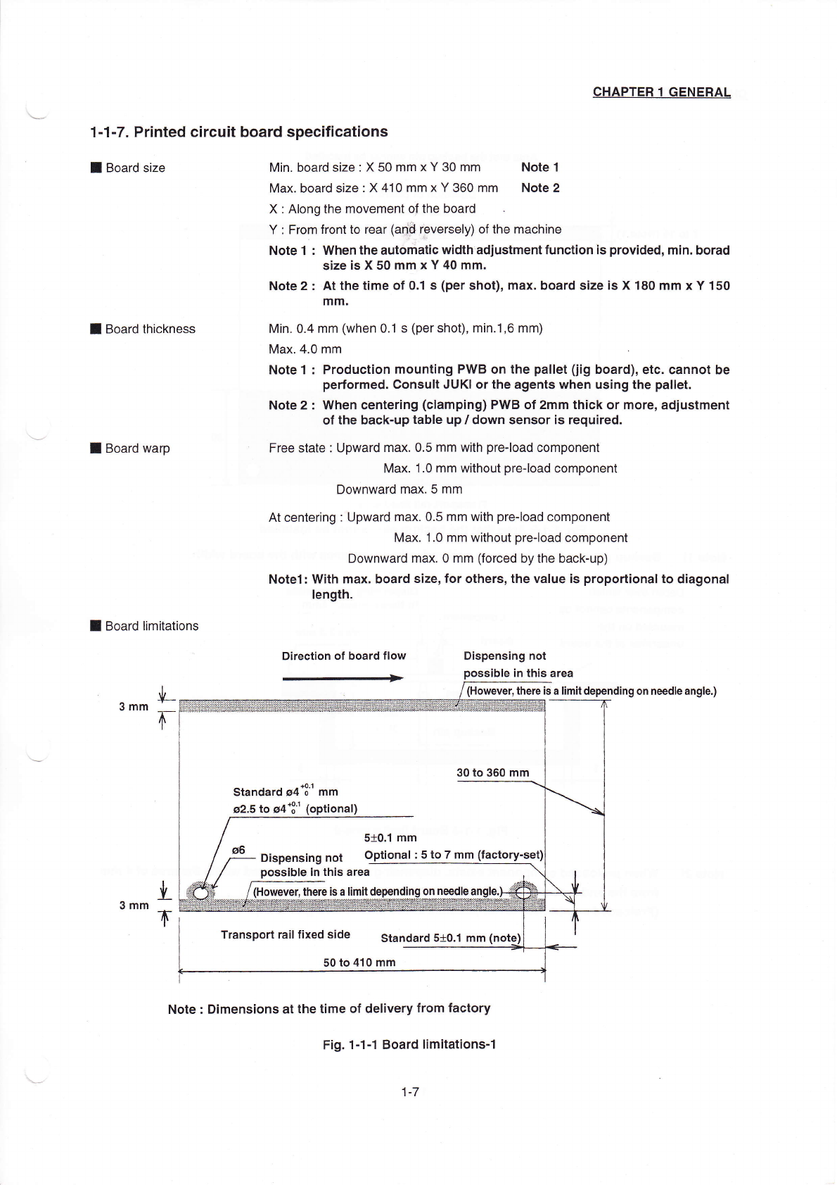
Direction of board flow
Dispensing not
p°
ssibIe in this area
(H。
wever,there‘
aⅡ
m"depending on n∞
dle angle,)
Transport ra"fixed side standard5±
0.1
50to410mm
Note:Dimensions atthe t"η
e of de"very from factory
Fig.,ˉ
1ˉ 1BOard I∶
mitationsˉ 1
¤2.5to g4喟
勺
¤6 Dispensing not op刂
onaI:5to7mm
lHOweve1there⒗
aⅡm1depending on n∞
dle
1ˉ 7
CHAPTER1GENERAL
■
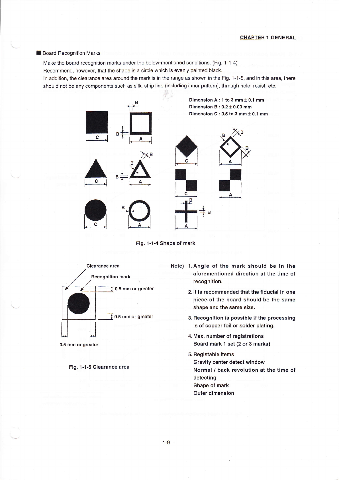
BOard Recognition Marks
Make the board recogn"ion rnarks underthe beIowˉ
mentioned cond"ions‘
(FIg,1ˉ
1ˉ 4)
Recommend,however,thatthe shape is a circIe which is evenIy painted black.
In addition,the Clearance area around the rη
ark is in the range as shown in the Fig.1ˉ
1ˉ
5,and in this area,there
should not be any components such as s"k,strip Iine(including inner pauern),through hole,resist,etC。
田mension A:1to3mm± 0.1mm
Dimension B:0.2±
0.03mm
Dirnension C:0.5to3mm± 0.丬 mm
F:g.1ˉ 1ˉ
4shape of mark
NOte) 1・ AngIe of the mark shouId be in the
aforement∶ oned direction at the time of
recogn;tion.
2."is reCoΠ 1mended thatthe fiduciaIin one
piece ofthe board should be the same
shape and the same size.
3.Recogn"ion∶
s possibIe ifthe processing
is of copperfo∶
I Or solder pIating.
4.Max。 number of registrations
Board mark1set(2°r3marks)
5.RegistabIe items
Gravity center detect window
Norma∶
'back revoIution at the time of
detecting
shape of mark
outer dimension
寺
:
o.s mm or greater
o.5mm or greater
o.5mm or greater
Fig.1ˉ
⒈5CIearance area
1-9