mi17050592.pdf - 第4页
Micromachines 2026 , 17 , 592 4 of 34 • Practical guidelines for algorithm selection based on operating regime and hyster e- sis conditions; • Systematic hyperparameter optimization of Bayesian algorithms between experim…

Micromachines 2026, 17, 592
3 of 34
This is a necessary evolution for high-volume scenarios: an integrated optical probe card
can save precious seconds per die in alignment, which compounded over hundreds of dies
yields substantial throughput gains [6,10,11].
Equally important, integrating the optical aligners into the probe hardware enables
parallel multi-channel testing. For instance, the Eclipse Dynamic (and similar systems)
can couple many fiber channels at once, leveraging parallel optical tests to further boost
throughput. Probe-card-based architectures that co-integrate optical and electrical inter-
faces are already enabling this parallelism [
5
,
12
], and recent fully automated wafer-level
systems demonstrate the viability of high-throughput multi-site electro-optical characteri-
zation [10].
Another key aspect of our solution is its cost-effective control strategy. High-
performance aligners often employ closed-loop feedback (using interferometric sensors
or strain gauges) to achieve nanometric precision and to counteract piezo hysteresis and
drift. Piezoelectric actuators inherently exhibit this hysteresis behavior, where displacement
depends not only on the applied voltage but also on the voltage history [
13
]. Because this
non-linearity is particularly pronounced at higher voltages, it can significantly impact
alignment accuracy and speed. However, implementing closed-loop control to mitigate this
in a dense multi-fiber probe head would add considerable complexity and cost. Instead,
the Eclipse Dynamic system exploits advanced open-loop control with algorithmic com-
pensation for these actuator nonlinearities. Furthermore, because each measurement point
requires time for actuator movement and signal settling, the choice of alignment algorithm
and operating speed regime plays a crucial role in determining overall testing throughput.
However, modern modeling techniques for piezoelectric actuators have made it feasi-
ble to achieve accuracies of a few nanometers without physical feedback sensors. Hysteresis
operators like the Preisach and Prandtl–Ishlinskii (P-I) model can be mathematically in-
verted for feedforward linearization of piezo stages [
14
,
15
]. Recent research has improved
upon these classical models to address rate-dependent and asymmetric hysteresis, using
modified P-I operators or even data-driven approaches (e.g., sparse and machine-learning-
based hysteresis models) for greater accuracy [
16
,
17
]. By leveraging such techniques, our
piezo actuators in the probe head are software-linearized, enabling repeatable sub-micron
alignments in open-loop. This avoids the need for embedded nano-position encoders
on each axis, thereby simplifying the probe hardware and enhancing robustness in a
production environment.
In this work, we present a comprehensive study of alignment optimization tech-
niques. We evaluate seven different alignment algorithms through both experimental
measurements and simulated data generated from experimental scans. Each algorithm was
evaluated across eight distinct on-wafer die locations (spanning multiple reticle positions)
directly on the Eclipse Dynamic hardware. Our analysis considers both high-speed (HS)
and low-speed (LS) operating regimes, as well as the impact of piezoelectric hysteresis on
alignment performance. Following best practices for algorithm comparison [
18
], we employ
data profile analysis rather than simple averaging to account for the non-normal distribu-
tion of convergence steps, particularly as the number of optimization problems increases.
The key contributions of this work can thus be listed as:
•
Comprehensive experimental characterization of seven alignment algorithms on eight
real wafer-level PIC coupling scenarios;
•
Simulation framework for generating synthetic alignment scenarios with controllable
hysteresis effects;
• Statistical analysis using data profiles for rigorous algorithm comparison;
•
Comparative performance evaluation across high-speed and low-speed operating
conditions;
https://doi.org/10.3390/mi17050592

Micromachines 2026, 17, 592
4 of 34
•
Practical guidelines for algorithm selection based on operating regime and hystere-
sis conditions;
•
Systematic hyperparameter optimization of Bayesian algorithms between experimen-
tal and simulation phases.
While the individual search algorithms utilized in this study are established numerical
methods, the core contribution of this work is their rigorous, system-level benchmarking
within the strict hardware constraints of industrial PIC testing. By evaluating these algo-
rithms under diverse operational extremes, we provide actionable guidelines for production
deployment. These algorithms are particularly vital for emerging coupling approaches,
such as 3D-printed edge couplers or micro-optics [
19
], where device-to-device spatial
variations are larger and demand highly robust dynamic active alignment.
The remainder of this paper is organized as follows: Section 2 reviews related work in
PIC testing and alignment optimization. Section 3 describes the Eclipse Dynamic system
and details the alignment algorithms under investigation. Section 4 presents experimental
and simulation results with data profile analysis. Section 5 discusses the comparative
performance and provides recommendations. Finally, Section 6 concludes the paper and
outlines future work.
2. Background
2.1. Wafer-Level Photonic Testing and Integrated Probe Head Architectures
Wafer-level testing of PICs has attracted growing attention, driven by the need to
validate optical performance at scale before costly packaging steps [
3
,
4
]. A central challenge
is related to achieving reliable, repeatable fiber-to-chip optical coupling across hundreds
of dies per wafer, each requiring sub-micron positional accuracy in multiple degrees of
freedom [
3
]. Early test setups relied on ad-hoc laboratory configurations in which skilled
operators manually aligned individual optical fibers using bench-top micro-positioners,
resulting in test times on the order of minutes per die and making high-volume charac-
terization practically infeasible [
4
]. The broader silicon photonics community has since
worked toward automated, reproducible measurement flows that integrate optical probing
with standard wafer probers [2,4].
A key architectural trend is the consolidation of optical and electrical probing into a
unified probe head compatible with conventional wafer probers, eliminating the need for
separate, bulky fiber positioning equipments. Two distinct philosophies have emerged.
The first relies on passive, alignment-insensitive optical coupling: by carefully engineering
the beam characteristics of the on-card optics, the positional tolerances of the prober chuck
become sufficient for adequate coupling without any per-die active correction, effectively
removing per-die alignment overhead and pushing throughput toward the electrical-
probing limit [
4
,
5
]. The second philosophy, adopted in the present work, retains active
micro-positioning of the FAU within the probe head using compact piezoelectric actuators,
allowing fine coupling optimization on each die and accommodating device-to-device
variation at the cost of a short, software-driven alignment routine per die [
7
,
8
]. Both
approaches represent a clear departure from external hexapod or gantry aligners attached
to the prober periphery, which added equipment cost, floor-space overhead, and limited
the degree of test parallelism achievable.
Probe-card-based solutions capable of parallel multi-channel measurements have been
demonstrated for a range of PIC types. Petrini et al. integrated a fiber-array probe with an
electrical card to enable simultaneous multi-channel characterization of photonic filters
without external positioning equipment [
5
]. Wu et al. demonstrated a butt-coupling probe
card with on-board polarization control, allowing polarization-sensitive PICs to be tested at
wafer scale without any separate fiber aligner [
12
]. Recent work by Jansen et al. presented
https://doi.org/10.3390/mi17050592
Micromachines 2026, 17, 592
5 of 34
a systematic optimization of optical alignment routines specific for high-throughput PIC
testing, confirming that algorithm selection has a direct and quantifiable impact on test
throughput and yield in production environments [
11
]. Fully automated edge-coupling
probers have further shown that optimized optical search routines and move sequences
can reduce per-die alignment time to the multi-second range, yielding throughputs on the
order of several thousand optical alignments per hour in single-fiber scenarios [10].
A complementary challenge, intimately linked to both alignment speed and precision,
concerns the motion stage itself. In automated PIC assembly and test, the demands for high
positioning precision and high throughput are fundamentally opposed: operating a motion
stage faster imposes higher control bandwidth requirements and degrades repeatability [
20
].
Mandelli et al. developed machine-learning models to predict motion stage precision as
a function of operating speed for PIC assembly systems, demonstrating that data-driven
approaches can characterize and compensate for these trade-offs without offline calibration
runs [
20
]. These findings directly motivate the evaluation of high-speed operating regimes
in the present work, and the need to understand how alignment algorithms degrade under
reduced repeatability conditions.
2.2. Optical Coupling Methods
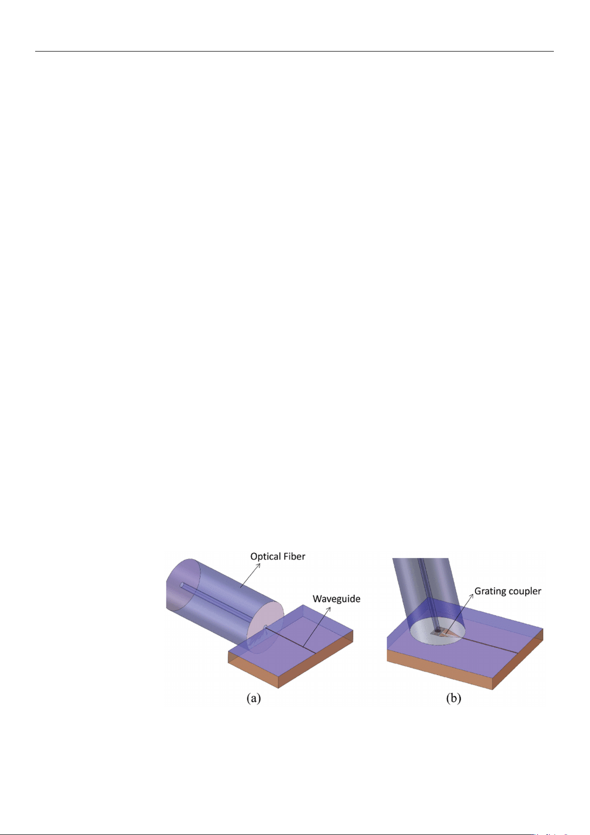
Two primary optical coupling architectures are relevant to wafer-level PIC testing,
as illustrated in Figure 1. As a foundational concept, edge couplers offer high coupling
efficiency and broad optical bandwidth by laterally aligning an optical fiber to the cleaved
or polished chip edge, requiring tight positional tolerances (typically below 1
µ
m) [
21
,
22
].
However, as illustrated conceptually in Figure 1a, pure lateral access is often physically
impossible in densely packed wafer-scale environments, necessitating the use of specialized
vertical-to-horizontal beam delivery tools. Grating couplers provide a more convenient
vertical-incidence interface compatible with full-wafer probing without edge preparation,
but at the expense of higher insertion loss, narrower wavelength bandwidth, and moderate
polarization sensitivity [23,24].
Most integrated probe card solutions for grating couplers rely either on external
positioning stages or on beam-expansion optics to reduce sensitivity to lateral misalignment,
the latter incurring an additional insertion-loss penalty [
25
]. The Eclipse Dynamic system
investigated here targets grating coupler interfaces, where the piezoelectric FAU provides
the fine positioning needed to maximize coupling efficiency across the full 15
µm ×
15
µm
scan range.
Figure 1. Schematic diagrams of the two primary optical coupling approaches: (a) traditional
horizontal edge coupling (which, for high-density wafer-level testing, is modified using micro-lenses
to allow vertical fiber access) and (b) Grating coupling [26].
https://doi.org/10.3390/mi17050592