mi17050592.pdf - 第5页
Micromachines 2026 , 17 , 592 5 of 34 a systematic optimization of optical alignment r outines specific for high-thr oughput PIC testing, confirming that algorithm selection has a direct and quantifiable impact on test thro…

Micromachines 2026, 17, 592
4 of 34
•
Practical guidelines for algorithm selection based on operating regime and hystere-
sis conditions;
•
Systematic hyperparameter optimization of Bayesian algorithms between experimen-
tal and simulation phases.
While the individual search algorithms utilized in this study are established numerical
methods, the core contribution of this work is their rigorous, system-level benchmarking
within the strict hardware constraints of industrial PIC testing. By evaluating these algo-
rithms under diverse operational extremes, we provide actionable guidelines for production
deployment. These algorithms are particularly vital for emerging coupling approaches,
such as 3D-printed edge couplers or micro-optics [
19
], where device-to-device spatial
variations are larger and demand highly robust dynamic active alignment.
The remainder of this paper is organized as follows: Section 2 reviews related work in
PIC testing and alignment optimization. Section 3 describes the Eclipse Dynamic system
and details the alignment algorithms under investigation. Section 4 presents experimental
and simulation results with data profile analysis. Section 5 discusses the comparative
performance and provides recommendations. Finally, Section 6 concludes the paper and
outlines future work.
2. Background
2.1. Wafer-Level Photonic Testing and Integrated Probe Head Architectures
Wafer-level testing of PICs has attracted growing attention, driven by the need to
validate optical performance at scale before costly packaging steps [
3
,
4
]. A central challenge
is related to achieving reliable, repeatable fiber-to-chip optical coupling across hundreds
of dies per wafer, each requiring sub-micron positional accuracy in multiple degrees of
freedom [
3
]. Early test setups relied on ad-hoc laboratory configurations in which skilled
operators manually aligned individual optical fibers using bench-top micro-positioners,
resulting in test times on the order of minutes per die and making high-volume charac-
terization practically infeasible [
4
]. The broader silicon photonics community has since
worked toward automated, reproducible measurement flows that integrate optical probing
with standard wafer probers [2,4].
A key architectural trend is the consolidation of optical and electrical probing into a
unified probe head compatible with conventional wafer probers, eliminating the need for
separate, bulky fiber positioning equipments. Two distinct philosophies have emerged.
The first relies on passive, alignment-insensitive optical coupling: by carefully engineering
the beam characteristics of the on-card optics, the positional tolerances of the prober chuck
become sufficient for adequate coupling without any per-die active correction, effectively
removing per-die alignment overhead and pushing throughput toward the electrical-
probing limit [
4
,
5
]. The second philosophy, adopted in the present work, retains active
micro-positioning of the FAU within the probe head using compact piezoelectric actuators,
allowing fine coupling optimization on each die and accommodating device-to-device
variation at the cost of a short, software-driven alignment routine per die [
7
,
8
]. Both
approaches represent a clear departure from external hexapod or gantry aligners attached
to the prober periphery, which added equipment cost, floor-space overhead, and limited
the degree of test parallelism achievable.
Probe-card-based solutions capable of parallel multi-channel measurements have been
demonstrated for a range of PIC types. Petrini et al. integrated a fiber-array probe with an
electrical card to enable simultaneous multi-channel characterization of photonic filters
without external positioning equipment [
5
]. Wu et al. demonstrated a butt-coupling probe
card with on-board polarization control, allowing polarization-sensitive PICs to be tested at
wafer scale without any separate fiber aligner [
12
]. Recent work by Jansen et al. presented
https://doi.org/10.3390/mi17050592
Micromachines 2026, 17, 592
5 of 34
a systematic optimization of optical alignment routines specific for high-throughput PIC
testing, confirming that algorithm selection has a direct and quantifiable impact on test
throughput and yield in production environments [
11
]. Fully automated edge-coupling
probers have further shown that optimized optical search routines and move sequences
can reduce per-die alignment time to the multi-second range, yielding throughputs on the
order of several thousand optical alignments per hour in single-fiber scenarios [10].
A complementary challenge, intimately linked to both alignment speed and precision,
concerns the motion stage itself. In automated PIC assembly and test, the demands for high
positioning precision and high throughput are fundamentally opposed: operating a motion
stage faster imposes higher control bandwidth requirements and degrades repeatability [
20
].
Mandelli et al. developed machine-learning models to predict motion stage precision as
a function of operating speed for PIC assembly systems, demonstrating that data-driven
approaches can characterize and compensate for these trade-offs without offline calibration
runs [
20
]. These findings directly motivate the evaluation of high-speed operating regimes
in the present work, and the need to understand how alignment algorithms degrade under
reduced repeatability conditions.
2.2. Optical Coupling Methods
Two primary optical coupling architectures are relevant to wafer-level PIC testing,
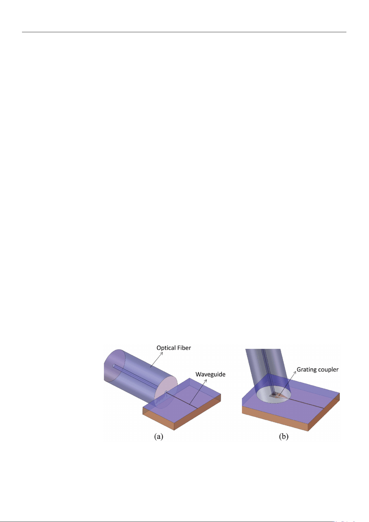
as illustrated in Figure 1. As a foundational concept, edge couplers offer high coupling
efficiency and broad optical bandwidth by laterally aligning an optical fiber to the cleaved
or polished chip edge, requiring tight positional tolerances (typically below 1
µ
m) [
21
,
22
].
However, as illustrated conceptually in Figure 1a, pure lateral access is often physically
impossible in densely packed wafer-scale environments, necessitating the use of specialized
vertical-to-horizontal beam delivery tools. Grating couplers provide a more convenient
vertical-incidence interface compatible with full-wafer probing without edge preparation,
but at the expense of higher insertion loss, narrower wavelength bandwidth, and moderate
polarization sensitivity [23,24].
Most integrated probe card solutions for grating couplers rely either on external
positioning stages or on beam-expansion optics to reduce sensitivity to lateral misalignment,
the latter incurring an additional insertion-loss penalty [
25
]. The Eclipse Dynamic system
investigated here targets grating coupler interfaces, where the piezoelectric FAU provides
the fine positioning needed to maximize coupling efficiency across the full 15
µm ×
15
µm
scan range.
Figure 1. Schematic diagrams of the two primary optical coupling approaches: (a) traditional
horizontal edge coupling (which, for high-density wafer-level testing, is modified using micro-lenses
to allow vertical fiber access) and (b) Grating coupling [26].
https://doi.org/10.3390/mi17050592

Micromachines 2026, 17, 592
6 of 34
2.3. Alignment Optimization Algorithms
The selection of the optical alignment search algorithm fundamentally determines
both the speed and the reliability of the per-die coupling step in photonic testing. Conven-
tional procedures have historically relied on brute-force scanning or iterative hill-climbing
techniques to locate the optimal coupling position. A typical approach involves raster or
spiral scanning, where the optical fiber is translated exhaustively across a multidimensional
grid until an initial optical signal is detected, followed by dense sweeps to map the cou-
pling efficiency landscape and identify the peak. Although robust to complex landscape
topologies, these exhaustive methods require a prohibitively large number of actuator
motions and power readings. Consequently, they can consume dozens of seconds for
a single alignment, making them impractical for high-volume manufacturing scenarios,
especially when multiple degrees of freedom are involved [
4
]. To mitigate this measure-
ment burden, cross-scan or dimensional-reduction approaches sequentially sweep along
individual axes to identify approximate peak coordinates before performing a focused local
refinement scan.
To further accelerate the alignment process, modern systems increasingly employ ad-
vanced optimization algorithms, such as gradient-based searches. These methods estimate
local coupling gradients, often through small dither motions, and steer the optical array in
the ascent direction to rapidly approach the optimum. Analogous to numerical gradient
descent or ascent, this targeted approach can converge significantly faster than blind scan-
ning. For instance, substituting a coarse spiral scan with an optimized gradient search has
been shown to yield an approximate 5
×
reduction in fiber coupling time [
10
]. Despite their
simplicity and speed, gradient methods are inherently susceptible to local maxima in the
measured optical power and require careful tuning of step-size parameters, particularly
when the coupling landscape contains secondary lobes or is distorted by actuator nonlin-
earities [
10
,
11
]. A central tension in these systems lies in balancing aggressive, adaptive
step sizes that yield the fastest convergence on benign landscapes against conservative,
fixed step sizes that maintain reliability on more challenging topologies.
As a powerful alternative, Bayesian optimization (BO) utilizing Gaussian Process (GP)
surrogates has emerged to address the limitations of both grid-based and gradient methods.
This approach treats the coupling yield as an unknown black-box function, building a
probabilistic surrogate model that is iteratively updated with each measurement [
27
].
By intelligently maximizing an acquisition function such as Expected Improvement, the
optimizer strategically balances the exploration of uncertain regions against the exploitation
of known high-power areas. This enables the algorithm to infer the global landscape
shape and locate optima using far fewer evaluations than traditional methods. Originally
popularized in complex domains like X-ray beamline autoalignment [
28
] and online control
of particle accelerators [
29
], BO excels in environments where the objective function is
expensive to evaluate and subject to noise. These characteristics are highly analogous
to optical power measurements affected by piezoelectric nonlinearities and mechanical
vibrations. Machine-learning-driven alignment has similarly demonstrated success in
multidimensional free-space optical systems and lens assemblies, proving the efficacy of
Bayesian algorithms in handling complex alignments with minimal iterations [30].
Within the BO family, two distinct paradigms are particularly relevant to the photonic
alignment problem. Global BO explores the entire search space from the outset, relying
purely on the GP posterior to select the next sampling location. While this maximizes
coverage and sample efficiency, it scales poorly with search-space dimensionality and can
be sensitive to landscape distortions introduced by actuator nonlinearities. Conversely,
local BO restricts the search to a neighborhood around a promising region identified by
an initial coarse scan. This restricted approach sidesteps the curse of dimensionality and
https://doi.org/10.3390/mi17050592