mi17050592.pdf - 第8页
Micromachines 2026 , 17 , 592 8 of 34 constant upon a reversal of dir ection until the input change exceeds a defined thr eshold width, after which the output linearly tracks the input. The P-I model is particularly notab…

Micromachines 2026, 17, 592
7 of 34
delivers strong empirical performance while maintaining rigorous convergence guaran-
tees [
31
]. Theoretical analyses have characterized the asymptotic behavior of local BO,
confirming conditions under which locally found stationary points closely approximate
the global optimum [
31
]. Furthermore, replacing standard gradient-descent exploitation
with a strategy that minimizes the upper confidence bound over the GP posterior yields
tighter theoretical guarantees and improved empirical results [
32
]. These theoretical ad-
vances directly motivate localized Bayesian strategies, which combine a coarse cross-scan
initialization with a focused GP refinement step.
Beyond the optimization of single-channel algorithms, the transition toward par-
allel, multi-channel alignment represents a critical advancement for wafer-level testing.
Because modern integrated probe architectures can simultaneously engage multiple in-
put and output fiber pairs across a die, applying alignment algorithms concurrently to
all channels drastically shortens the overall test time. Aligning channels sequentially is
highly inefficient; instead, coordinated multi-dimensional searches that optimize all optical
ports together are essential for maximizing throughput. Ultimately, the field is rapidly
transitioning from simplistic single-variable scans toward intelligent, multi-variable, and
machine-learning-augmented optimizations. Through the integration of these advanced
algorithmic approaches, the optical alignment step can be reduced to a minor fraction of
the total test time, making active alignment on the scale of a few seconds a viable reality for
high-volume production.
2.4. Hysteresis and Nonlinearity Compensation
Piezoelectric actuators are extensively utilized in nanometric alignment systems due
to their high resolution and rapid response times. However, a persistent challenge is their
inherent hysteresis and creep. The displacement produced by the actuator at a given
drive voltage depends not only on that specific voltage but on the entire preceding voltage
history, a phenomenon driven by domain-wall motion and polarization switching within
the piezoelectric ceramic [
13
]. In open-loop operation, this path-dependent nonlinearity
typically introduces positioning errors spanning 10–15% of the total travel range [
33
]. Such
substantial deviations far exceed the strict sub-micron tolerances required for reliable
fiber-to-waveguide alignment in PICs.
The traditional remedy for addressing hysteresis is closed-loop control. By integrating
an embedded feedback sensor such as a capacitive sensor, strain gauge, or linear variable
differential transformer (LVDT), and utilizing PID or iterative control, systems can dynami-
cally correct positioning errors to achieve sub-nanometer accuracy. While highly effective,
closed-loop architectures introduce significant drawbacks: they are more expensive, impose
bandwidth limitations, and add substantial hardware complexity. For dense, multi-channel
probe heads (e.g., a 16-channel array), embedding a dedicated physical sensor and its asso-
ciated wiring on every piezoelectric axis is highly impractical. Position sensors, moreover,
require space for installation that is not available in the application hereby discussed.
To circumvent these hardware limitations, the preferred strategy is open-loop control
enhanced by software-based feedforward compensation algorithms. By characterizing the
hysteresis behavior of the piezo and applying an inverse model to the drive signals, the
response of the actuator can be effectively linearized. This software-driven approach scales
effortlessly across several channels without the prohibitive overhead of extra hardware.
Over the past two decades, various frameworks have been developed to model and com-
pensate for piezoelectric hysteresis. Classical approaches include the Preisach model, which
captures hysteresis through a superposition of elementary bistable operators, and the P-I
model, which employs a weighted sum of play operators [
14
,
15
]. Conceptually, a play
operator acts as a mathematical representation of mechanical backlash: its output remains
https://doi.org/10.3390/mi17050592

Micromachines 2026, 17, 592
8 of 34
constant upon a reversal of direction until the input change exceeds a defined threshold
width, after which the output linearly tracks the input. The P-I model is particularly notable
because it admits an analytical inverse that can be cascaded with the physical actuator as a
feedforward pre-distortion signal to yield a linear response.
To handle more complex behaviors like asymmetric hysteresis, saturation, and rate de-
pendence, advanced direct-inverse and modified approaches have been developed [
16
,
34
].
For example, classical symmetric P-I play operators, which apply the exact same threshold
and slope regardless of whether the voltage is increasing or decreasing, struggle to capture
the divergent ascending and descending branches of physical piezoceramics. Utilizing
modified asymmetric play operators, which assign distinct mathematical characteristics
to the forward and return paths, allows for a more accurate description of this directional
behavior with fewer model parameters [
35
]. Furthermore, while the classical P-I model
possesses a straightforward analytical inverse, utilizing the aforementioned modified mod-
els often introduces complex mathematical inversions that are computationally heavy for
real-time control. To resolve this, Gu et al. demonstrated a direct-inverse compensation
method that characterizes the inverse hysteresis effect directly, bypassing these heavy
calculations and achieving tracking error reductions of up to 90% [
36
]. Similarly, Yu et al.
utilized a rate-dependent modified P-I model to reduce linear positioning errors from 10%
to below 1% [33].
More recently, data-driven methods have emerged as a powerful alternative. Ma-
chine learning approaches, such as the sparse system identification method proposed by
Chandra et al., can discover hysteresis models for specific piezo materials, demonstrating
residual strain errors well below 1%, which stands as a performance that rivals closed-loop
systems [
17
]. Ultimately, the viability of these various feedforward P-I linearization tech-
niques has been successfully validated in multi-axis optical alignment stages [
37
,
38
]. In
our implemented system, we calibrate each piezo axis using a variant of the P-I model. By
applying a series of voltage trajectories and recording the displacement via an external laser
sensor during the calibration phase, we identify the exact hysteresis curve. This model is
then inverted in real time by the controller to pre-distort commanded moves. Additionally,
a drift compensation table is applied via software to administer small, time-based offset
adjustments that counteract the slow creep occurring after a step maneuver.
Crucially, the impact of hysteresis extends beyond spatial accuracy; it introduces a
significant temporal penalty. When an alignment algorithm commands a move to a lower
voltage position, the system must perform a reset-to-zero maneuver to ensure the actuator
remains on the well-characterized forward path, rather than traversing an unpredictable
return path. This reset requirement fundamentally differentiates the movement overhead
of various search algorithms. Methods that frequently require downward voltage moves,
such as Bayesian algorithms that prioritize broad exploration before exploitation, incur a
disproportionate time penalty compared to monotone hill-climbing strategies. Understand-
ing how this temporal penalty interacts with the specific search strategy of each algorithm
across different operating speeds is a key contribution of this work. As our results in
Section 4 will demonstrate, this carefully implemented open-loop strategy reliably aligns
fibers with optical loss repeatability greater than 0.1 dB, validating that an algorithmic
approach to hysteresis can successfully meet the nanometric tolerances of high-volume
wafer-level photonic testing.
2.5. Algorithm Comparison Methodology
Traditional algorithm comparison often relies on averaging performance metrics such
as number of function evaluations or convergence time. However, as noted by Beiranvand
et al. [
18
], this approach can be misleading when the distribution of performance metrics is
https://doi.org/10.3390/mi17050592
Micromachines 2026, 17, 592
9 of 34
non-normal, particularly as the number of optimization problems increases. They advocate
for more rigorous statistical approaches including performance profiles and data profiles.
Performance profiles [
39
] measure the fraction of problems solved within a given
performance ratio relative to the best solver. Data profiles [
40
] extend this concept by
plotting the fraction of problems solved as a function of the number of function evaluations,
providing insight into convergence speed and robustness. These profile-based methods are
particularly appropriate for optimization algorithm comparison, as they account for the
full distribution of performance rather than relying on potentially misleading averages.
3. Methodology
3.1. Eclipse Dynamic System Architecture
To address the severe spatial constraints associated with conventional lateral edge
coupling in high-density wafer-level environments, the Eclipse Dynamic system employs
lensed fibers and 3D-printed micro-lenses [
19
] to redirect the optical signal from horizontal
propagation to vertical access. This configuration enables dense wafer-level probing while
remaining compatible with standard prober geometries and integrated electro-optical
test operation.
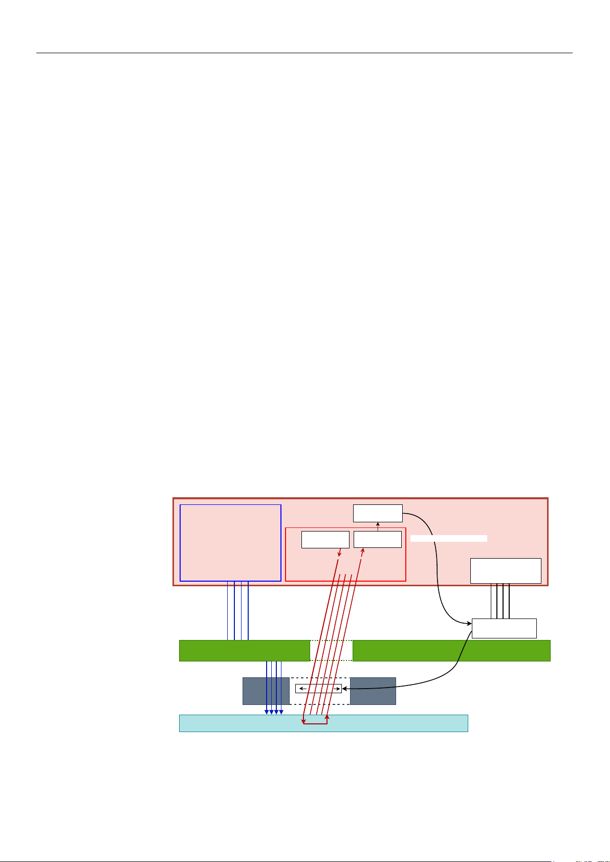
Figure 2 presents the system-level architecture of the Eclipse Dynamic probe card
during wafer-level testing. The tester provides both the electrical test program and the
optical test program. The optical path comprises a source/modulation stage and a detection
stage connected to the integrated FAU in the probe head, while the mechanical alignment
loop is closed through the controller and the piezoelectric drive electronics. The FAU
is integrated into the probe head together with the electrical probes, such that optical
and electrical contact are established on the same wafer site during probing. Rather than
actuating individual fibers independently, the system displaces the entire FAU as a single
rigid body in the X–Y plane, with differential actuation used for tilt compensation. This
architecture eliminates the need for external optical positioning stages and enables compact,
high-throughput wafer-level electro-optical testing.
Electrical Test
Testing program
Optical Test
Testing program
Optical
Modulator
Photoelectric
Converter
Optical Alignment Algorithm
Controller
Piezo Power Supplier
Piezo Voltage Boost
Probe Head
Align loop
Fiber Array Unit
PCB
Tester
Piezo
Wafer
Probes
Figure 2. System-level block diagram of the automated wafer-level photonic testing platform, show-
ing the tester, controller, optical source/detection chain, piezoelectric drive electronics, integrated
probe head, and wafer under test.
https://doi.org/10.3390/mi17050592