Maintenance Manual.pdf - 第80页
RL131 MAINTENANCE MANUAL 4.1 Control S ystem Conf iguration DA8MEC-14-020- A0 4.1-1 1 4.1.6 I/O Map I / O M AP INPUT Board connector Address No. Name bit Note 1 Right rail traverse limit 0 2 Right rail return l imit 1 3 …
RL131
MAINTENANCE MANUAL
4.1 Control System Configuration
DA8MEC-14-020-A0
4.1-10
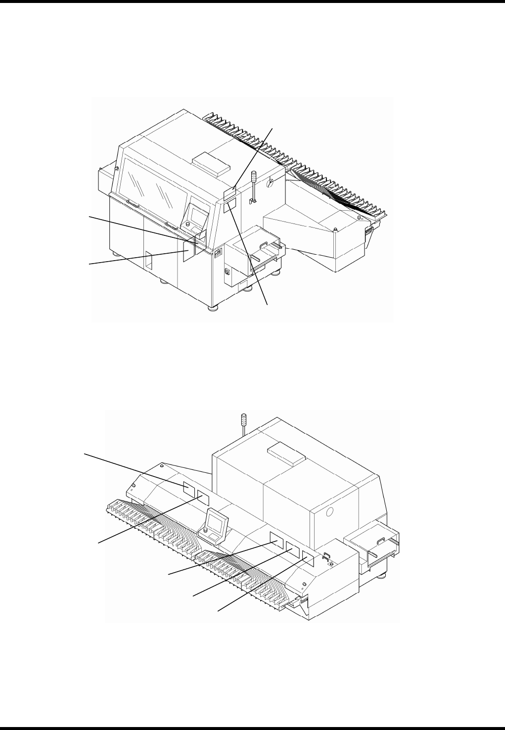
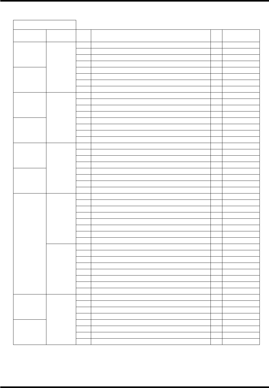
4.1.5 Ring I/O Load Board Arrangement
K311
K310
K333
K323
K326
K325
K324
K322
K327
RL131
MAINTENANCE MANUAL
4.1 Control System Configuration
DA8MEC-14-020-A0
4.1-11
4.1.6 I/O Map
I / O MAP INPUT
Board
connector
Address
No.
Name bit
Note
1
Right rail traverse limit 0
2
Right rail return limit 1
3
PCB detection 1 2
#0_CN16
4
PCB detection 2 3
5
Carry arm return detection 4
6
Carry arm slow down detection 5
7
Carry arm traverse detection 6
#0_CN15
0000
8
7
9
Main frame left side fan alarm 0
10
Main frame controller fan alarm 1
11
Main frame right side fan alarm 2
#0_CN14
12
3
13
4
14
5
15
6
#0_CN13
0001
16
7
17
0
18
1
19
2
#0_CN12
20
3
21
MLP input signal 4
Option
22
Air down 5
23
6
#0_CN11
0002
24
7
25
XY table inside PCB detection 0
26
Positioner error detection 1
27
XY table inside PCB detection 2 2
Option
28
2 PCB transfer 3
Option
29
Positioner lever traverse limit 4
30
Positioner lever return limit 5
31
6
0003
32
7
33
X AXIS+LIMIT 0
34
X AXIS ORG. 1
35
X AXIS-LIMIT 2
36
3
37
Y AXIS+LIMIT 4
38
Y AXIS ORG. 5
39
Y AXIS-LIMIT 6
#0_CN10
0004
40
7
41
Front cover detection 0
42
1
43
Push arm / push up traverse limit 2
Option
#1_CN16
44
Push arm / push up return limit 3
Option
45
Left rail traverse limit 4
46
Left rail return limit 5
47
PCB detection 3 6
#1_CN15
0040
48
PCB detection 4 7
RL131
MAINTENANCE MANUAL
4.1 Control System Configuration
DA8MEC-14-020-A0
4.1-12
I / O MAP INPUT
Board
connector
Address
No.
Name bit
Note
49
0
50
1
51
2
#1_CN14
52
3
53
qA AXIS+LIMIT
4
54
qA AXIS ORG.
5
55
qA AXIS-LIMIT
6
#1_CN13
0041
56
7
57
Insertion check 1 0
58
Insertion check 2 1
59
Insertion check 3 2
#1_CN12
60
Insertion check 4 3
61
4
62
5
63
Invertor run signal 6
#1_CN11
0042
64
Invertor abnormal signal 7
65
ZR change SW 0
66
1
67
2
68
3
69
4
70
5
71
6
0043
72
7
#1_CN10
0044 73
0
161
0
162
1
163
2
#4_CN14
164
3
165
CVT check 1 4
Option
166
CVT check 2 5
Option
167
6
#4_CN13
0101
168
7
169
PCB request delay 0
Option
170
PCB supply delay 1
Option
171
2
#4_CN12
172
3
173
4
174
5
175
6
#4_CN11
0102
176
7