00191017-01.pdf - 第517页
User ’s Manual Line Computer UNIX 17.3 Description of Components and P CBs Software V e rsion 403.xx Ed ition 06/97 17.3.1 PCB 1: single circuit 17 - 1 9 39. On the FILE menu cl ick on the Quit option. The F iducial Edit…
17.3 Description of Components and PCBs User’s Manual Line Computer UNIX
17.3.1 PCB 1: single circuit Software Version 403.xx Edition 06/97
17 - 18
No ink spot present.
No clusters and single circuits
present.
FILE
Save
FILE
Quit
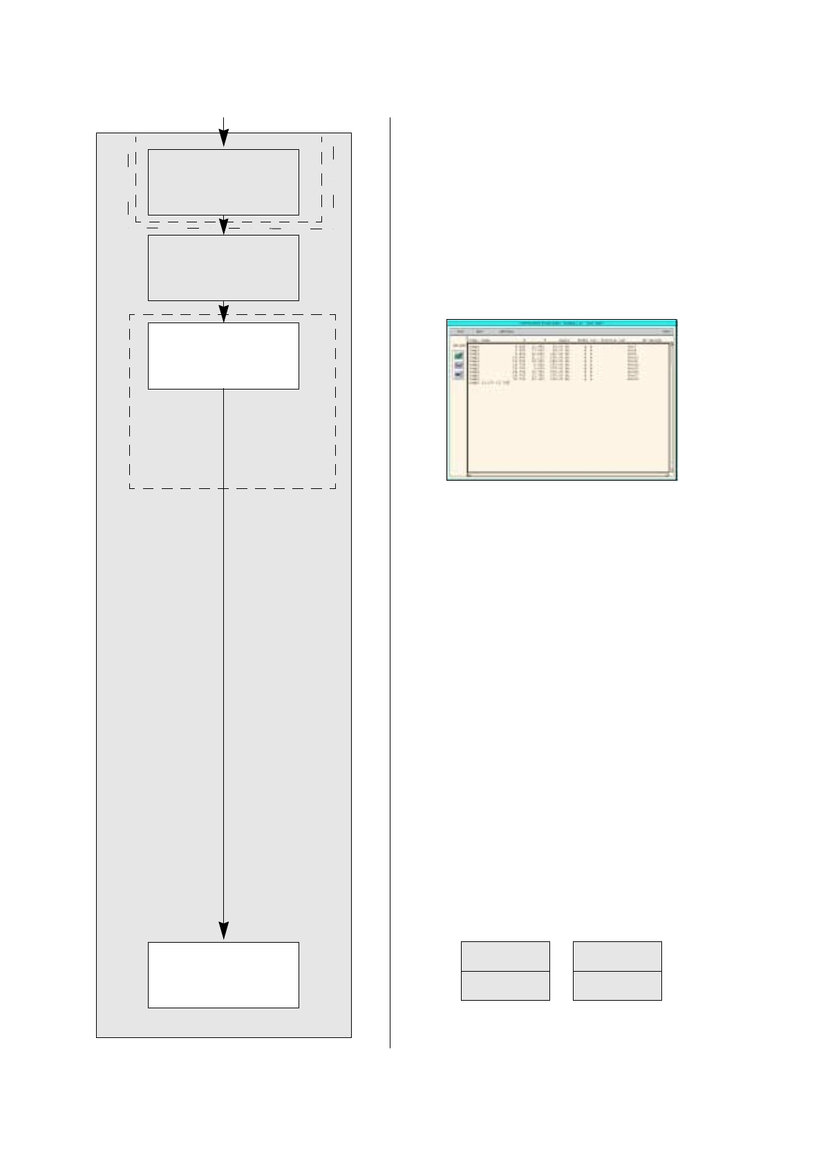
Entering placement
positions
Defining ink spot
Saving PCB data
Creating clusters and
single circuits
continued from page 17-16
PCB Description
Placement Position Editor
User’s Manual Line Computer UNIX 17.3 Description of Components and PCBs
Software Version 403.xx Edition 06/97 17.3.1 PCB 1: single circuit
17 - 19
39. On the
FILE
menu click on the
Quit
option.
The Fiducial Editor is closed.
40. In the Cluster Editor click on the
Quit
option on the
FILE
menu.
The Cluster Editor is closed.
Defining ink spot:
non ink spot present.
Creating clusters and single circuits:
no clusters and single circuits present.
To enter placement positions, proceed as follows:
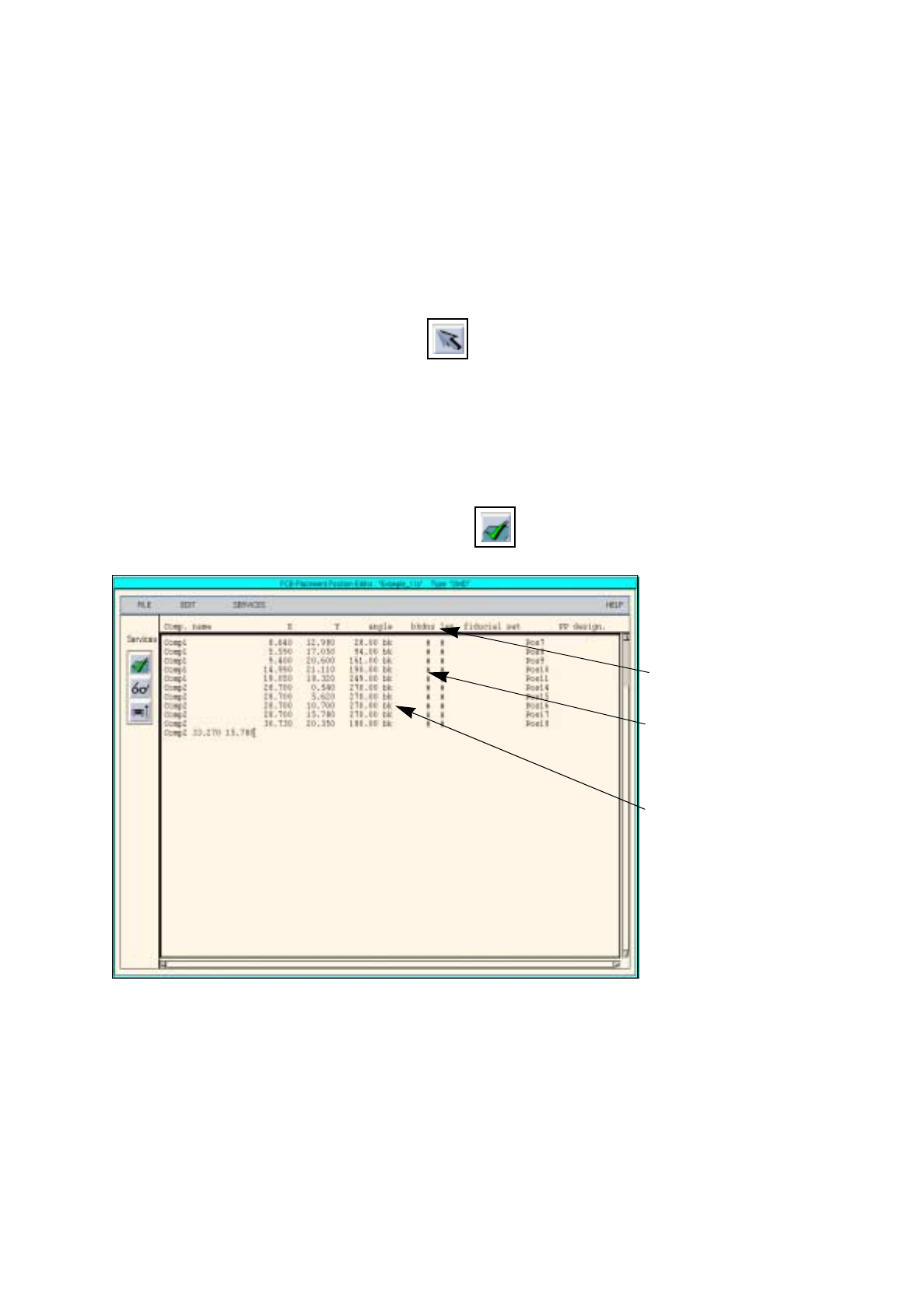
41. In the PCB Editor activate the Select icon .
42. Click on the PCB (rectangle).
The rectangle is highlighted in green.
43. On the
SERVICES
menu click on the
Placement Position Editor...
option.
The Placement Position Editor is opened.
44. Position the cursor in the entry field and enter placement positions in accordance with
Section Tab. 17.3-
2
. The
individual entries are to be separated by a blank. Confirm each line by pressing the Enter key.
45. When entry is complete, activate the Check icon .
The entered values are checked and arranged in columns (see
Fig. 17.3.3
).
Fig. 17.3.3 Placement Position Editor for PCB 1
46. Click on the
Quit
option on the
FILE
menu.
The Placement Position Editor is closed.
To save the PCB data, proceed as follows:
47. In the PCB Editor, click on the
Save
option on the
FILE
menu.
The PCB data are now saved.
48. On the
FILE
menu click on the
Quit
option.
Enter fiducial set name
# = no fiducials defined for the
placement position
b = placing
k = glueing
d = dispensing (solder paste)
n = reworking
s = blocking (from placement)
Enter number of placement
level
# = no level defined for the pla-
cement position
17.3 Description of Components and PCBs User’s Manual Line Computer UNIX
17.3.2 PCB 2: Focus on Package Form Description Software Version 403.xx Edition 06/97
17 - 20
PM1
PM2
PM3
Ink spot
PCB zero
40
96
5
5
30
86
15
17.3.2 PCB 2: Focus on Package Form Description
PCB 2 is a single circuit with three different components.
The package forms are not contained in the GF-Bibliothek, they must be newly described. For this purpose,
the package form numbers ranging from 1501 to 32767 of the customer GF-Bibliothek can be used.
The PCB is screen-printed, the components are only to be placed. No CRDL-test is envisaged. PCB position
recognition is to be performed; for this purpose three fiducials (PM) are available. An ink spot is also present.
The components at issue are one PDC, one regular FDC and one irregular FDC. The components are picked
up from the 0°-position.
Comp.name X Y Angle Comment
Comp4 0.00 61.00 0.00 Pos1
Comp4 10.00 61.00 0.00 Pos2
Comp4 20.00 61.00 0.00 Pos3
Comp4 30.00 61.00 0.00 Pos4
Comp4 0.00 51.00 0.00 Pos5
Comp4 10.00 51.00 0.00 Pos6
Comp4 20.00 51.00 0.00 Pos7
Comp4 30.00 51.00 0.00 Pos8
Comp4 0.00 41.00 0.00 Pos9
Comp4 10.00 41.00 0.00 Pos10
Tab. 17.3-3 Placement Positions of PCB 2
Comp4 20.00 41.00 0.00 Pos11
Comp4 30.00 41.00 0.00 Pos12
Comp4 0.00 31.00 0.00 Pos13
Comp4 10.00 31.00 0.00 Pos14
Comp4 20.00 31.00 0.00 Pos15
Comp4 30.00 31.00 0.00 Pos16
Comp5 15.00 81.00 0.00 Pos17
Comp5 15.00 71.00 0.00 Pos18
Comp6 5.00 10.00 -90.00 Pos19
Comp6 25.00 10.00 -90.00 Pos20
Comp.name X Y Angle Comment
Direction of travel
X
Y
PCB coordinate system 0°
PCB height= 1.5 mm
Corner
Fig. 17.3.4 Dimensions of PCB 2
Corner