multifunction-rio-user-manual.pdf - 第11页
Chapter 1 Introduction Multifunction Reconfigur able I/O User Manual 1-2 ni.com functionality of your device. If you only have LabVIEW b ut not the FPGA Module, you cannot create ne w FPGA VIs, but you can create VIs tha…

© National Instruments Corporation 1-1 Multifunction Reconfigurable I/O User Manual
1
Introduction
This chapter describes the concept and features of the Reconfigurable I/O
(RIO) devices, optional software and equipment, and safety information.
About the Reconfigurable I/O Device
Table 1-1 lists an overview of the NI 78xx Multifunction Reconfigurable
I/O devices.
A user-reconfigurable FPGA (Field-Programmable Gate Array) controls
the digital I/O lines on the PCI/PXI-781x, and the digital and analog I/O
lines on the device. The FPGA on your device allows you to define the
functionality and timing of the device. You can change the functionality of
the FPGA on your device in LabVIEW using the LabVIEW FPGA Module
to create and download a custom virtual instrument (VI) to the FPGA.
Using the FPGA Module, you can graphically design the timing and
Table 1-1. NI 78xx devices Multifunction RIO Device Overview
Device I/O Channels FPGA AI Sample Rate
PCI/PXI-7811 160 DIO Virtex-II XC2V1000 —
PCI/PXI-7813 160 DIO Virtex-II XC2V3000 —
PCI/PXI-7830 4 AI, 4 AO, 56 DIO Virtex-II XC2V1000 200 kS/s
PCI/PXI-7831 8 AI, 8 AO, 96 DIO Virtex-II XC2V1000 200 kS/s
PCI/PXI-7833 8 AI, 8 AO, 96 DIO Virtex-II XC2V3000 200 kS/s
PCIe/PXI-7841 8 AI, 8 AO, 96 DIO Virtex-5 LX30 200 kS/s
PCIe/PXI-7842 8 AI, 8 AO, 96 DIO Virtex-5 LX50 200 kS/s
PCIe/PXI-7851 8 AI, 8 AO, 96 DIO Virtex-5 LX30 750 kS/s
PCIe/PXI-7852 8 AI, 8 AO, 96 DIO Virtex-5 LX50 750 kS/s
PXI-7853 8 AI, 8 AO, 96 DIO Virtex-5 LX85 750 kS/s
PXI-7854 8 AI, 8 AO, 96 DIO Virtex-5 LX110 750 kS/s

Chapter 1 Introduction
Multifunction Reconfigurable I/O User Manual 1-2 ni.com
functionality of your device. If you only have LabVIEW but not the FPGA
Module, you cannot create new FPGA VIs, but you can create VIs that run
on Windows or a LabVIEW Real-Time (RT) target to control existing
FPGA VIs.
Some applications require tasks such as real-time, floating-point
processing or datalogging while performing I/O and logic on the device.
You can use the LabVIEW Real-Time Module to perform these additional
applications while communicating with and controlling your device.
The device contains Flash memory to store a startup VI for automatic
loading of the FPGA when the system is powered on.
The device uses the Real-Time System Integration (RTSI) bus to easily
synchronize several measurement functions to a common trigger or timing
event. PCI devices access the RTSI bus through a RTSI cable connected
between devices. PXI devices access the RTSI bus through the PXI trigger
lines implemented on the PXI backplane.
Refer to the Multifunction Reconfigurable I/O Specifications, available at
ni.com/docs, for detailed device specifications.
Using PXI with CompactPCI
Using PXI-compatible products with standard CompactPCI products is an
important feature provided by PXI Hardware Specification Revision 2.1
and PXI Software Specification Revision 2.1. If you use a PXI-compatible
plug-in card in a standard CompactPCI chassis, you cannot use
PXI-specific functions, but you still can use the basic plug-in card
functions. For example, the RTSI bus on the R Series device is available
in a PXI chassis but not in a CompactPCI chassis.
The CompactPCI specification permits vendors to develop sub-buses that
coexist with the basic PCI interface on the CompactPCI bus. Compatible
operation is not guaranteed between CompactPCI devices with different
sub-buses nor between CompactPCI devices with sub-buses and PXI.
The standard implementation for CompactPCI does not include these
sub-buses. The device works in any standard CompactPCI chassis adhering
to the PICMG CompactPCI 2.0 R3.0 core specification.
PXI-specific features are implemented on the J2 connector of the
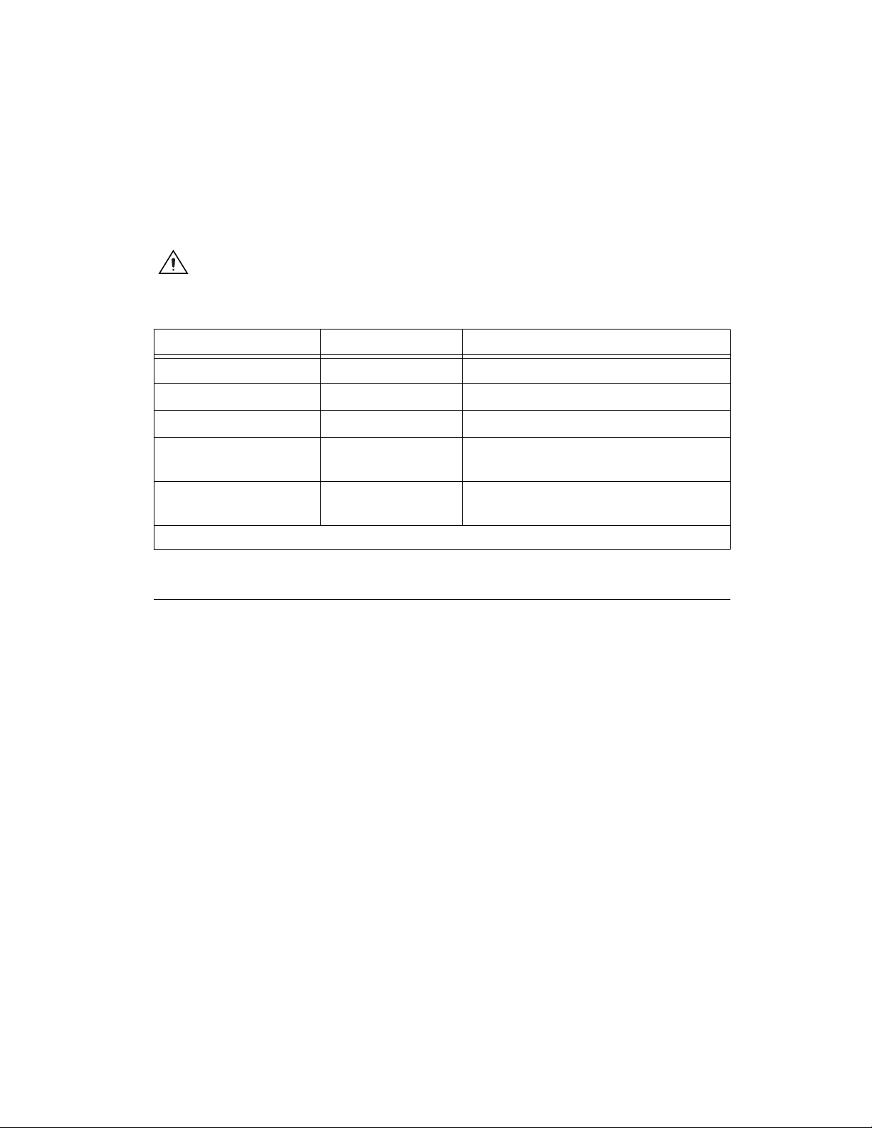
CompactPCI bus. Table 1-2 lists the J2 pins used by the PXI-78xx. The
NI 78xx is compatible with any CompactPCI chassis with a sub-bus that
Chapter 1 Introduction
© National Instruments Corporation 1-3 Multifunction Reconfigurable I/O User Manual
does not drive these lines. Even if the sub-bus is capable of driving these
lines, the device is still compatible as long as those pins on the sub-bus are
disabled by default and are never enabled.
Caution Damage can result if the J2 lines are driven by the sub-bus.
Overview of Reconfigurable I/O
This section explains reconfigurable I/O and describes how to use the
LabVIEW FPGA Module to build high-level functions in hardware.
Refer to Chapter 2, Hardware Overview of the NI 78xx, for descriptions of
the I/O resources on the NI 78xx.
Reconfigurable I/O Concept
Multifunction Reconfigurable I/O devices are based on a reconfigurable
FPGA core surrounded by fixed I/O resources for analog and digital input
and output. You can configure the behavior of the reconfigurable FPGA to
match the requirements of the measurement and control system. You can
implement this user-defined behavior as an FPGA VI to create an
application-specific I/O device.
Table 1-2. Pins Used by the NI 78xx
PXI-78xx Signal PXI Pin Name PXI J2 Pin Number
PXI_Trig<0..7> PXI Trigger<0..7> A16, A17, A18, B16, B18, C18, E16, E18
PXI_Clk10 PXI Clock 10 MHz E17
PXI_Star PXI Star Trigger D17
PXI_Lbl<0..12>
*
LBL<0..12> A1, A19, C1, C19, C20, D1, D2, D15, D19,
E1, E2, E19, E20
PXI_Lbr<0..12>
*
LBR<0..12> A2, A3, A20, A21, B2, B20, C3, C21,
D3, D21, E3, E15, E21
*
PXI-781x/783x only