multifunction-rio-user-manual.pdf - 第13页
Chapter 1 Introduction Multifunction Reconfigur able I/O User Manual 1-4 ni.com Flexible Functionality Flexible functiona lity allows the device to match ind ividual application requirements and t o mimic th e functional…
Chapter 1 Introduction
© National Instruments Corporation 1-3 Multifunction Reconfigurable I/O User Manual
does not drive these lines. Even if the sub-bus is capable of driving these
lines, the device is still compatible as long as those pins on the sub-bus are
disabled by default and are never enabled.
Caution Damage can result if the J2 lines are driven by the sub-bus.
Overview of Reconfigurable I/O
This section explains reconfigurable I/O and describes how to use the
LabVIEW FPGA Module to build high-level functions in hardware.
Refer to Chapter 2, Hardware Overview of the NI 78xx, for descriptions of
the I/O resources on the NI 78xx.
Reconfigurable I/O Concept
Multifunction Reconfigurable I/O devices are based on a reconfigurable
FPGA core surrounded by fixed I/O resources for analog and digital input
and output. You can configure the behavior of the reconfigurable FPGA to
match the requirements of the measurement and control system. You can
implement this user-defined behavior as an FPGA VI to create an
application-specific I/O device.
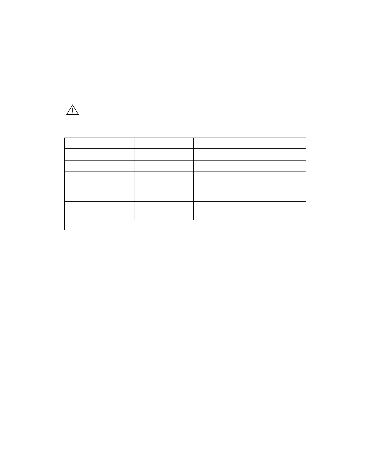
Table 1-2. Pins Used by the NI 78xx
PXI-78xx Signal PXI Pin Name PXI J2 Pin Number
PXI_Trig<0..7> PXI Trigger<0..7> A16, A17, A18, B16, B18, C18, E16, E18
PXI_Clk10 PXI Clock 10 MHz E17
PXI_Star PXI Star Trigger D17
PXI_Lbl<0..12>
*
LBL<0..12> A1, A19, C1, C19, C20, D1, D2, D15, D19,
E1, E2, E19, E20
PXI_Lbr<0..12>
*
LBR<0..12> A2, A3, A20, A21, B2, B20, C3, C21,
D3, D21, E3, E15, E21
*
PXI-781x/783x only

Chapter 1 Introduction
Multifunction Reconfigurable I/O User Manual 1-4 ni.com
Flexible Functionality
Flexible functionality allows the device to match individual application
requirements and to mimic the functionality of fixed I/O devices. For
example, you can configure a device in one application for three 32-bit
quadrature encoders and then reconfigure the device in another application
for eight 16-bit event counters.
You also can use the device with the LabVIEW Real-Time Module in
timing and triggering applications, such as control and
hardware-in-the-loop (HIL) simulations. For example, you can configure
the device for a single timed loop in one application and then reconfigure
the device in another application for four independent timed loops with
separate I/O resources.
User-Defined I/O Resources
You can create your own custom measurements using the fixed I/O
resources. For example, one application might require an event counter that
increments when a rising edge appears on any of three digital input lines.
With a PCI/PCIe/PXI-783x/784x/785x device, another application might
require a digital line to be asserted after an analog input exceeds a
programmable threshold. You can implement these behaviors in the
hardware for fast, deterministic performance.
Device-Embedded Logic and Processing
You can implement LabVIEW logic and processing in the FPGA of your
device. Typical logic functions include Boolean operations, comparisons,
and basic mathematical operations. You can implement multiple functions
efficiently in the same design, operating sequentially or in parallel. You
also can implement more complex algorithms such as control loops. You
are limited only by the size of the FPGA.
Chapter 1 Introduction
© National Instruments Corporation 1-5 Multifunction Reconfigurable I/O User Manual
Reconfigurable I/O Architecture
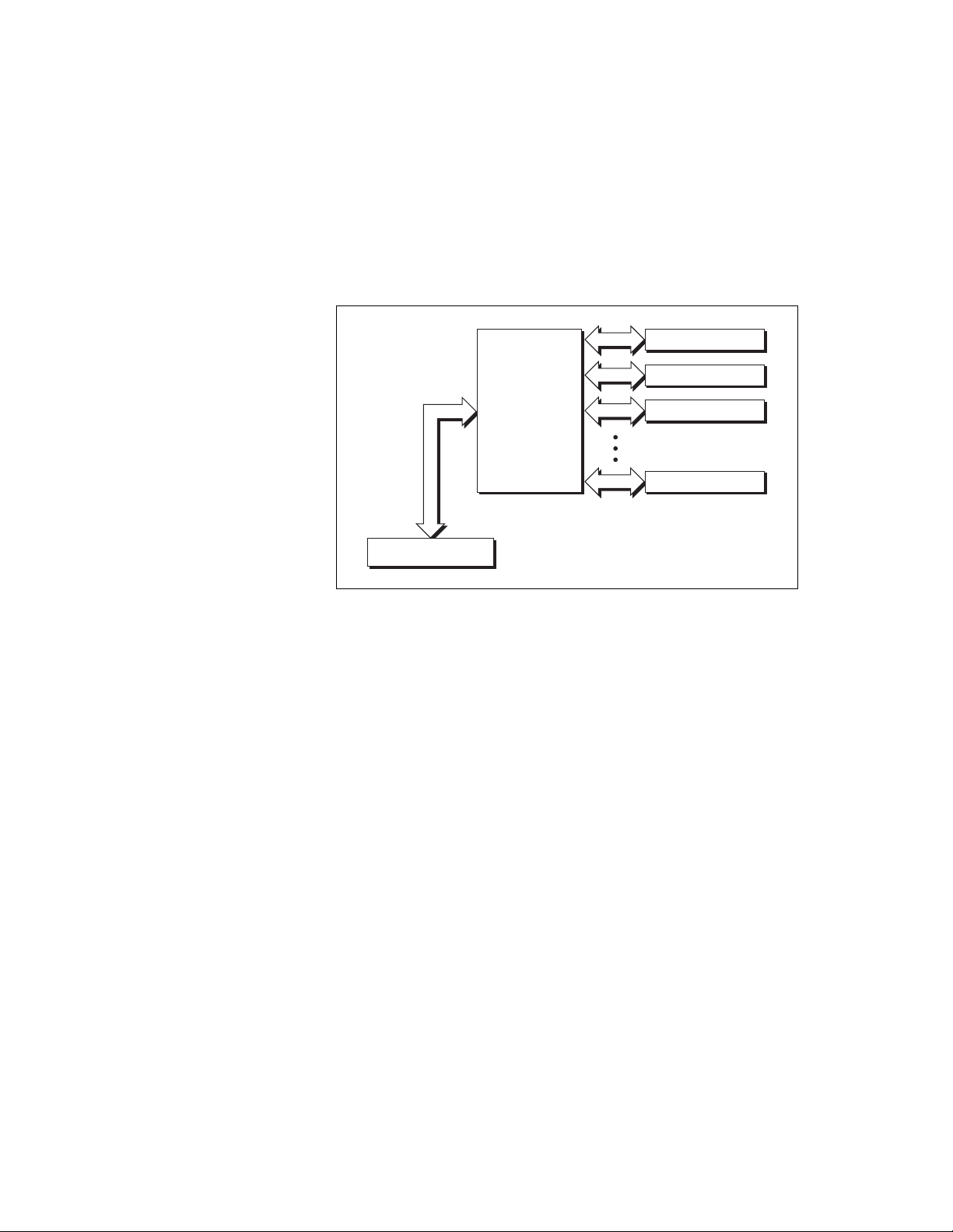
Figure 1-1 shows an FPGA connected to fixed I/O resources and a bus
interface. The fixed I/O resources include A/D converters (ADCs),
D/A converters (DACs), and digital I/O lines.
Figure 1-1. High-Level FPGA Functional Overview
Software accesses the device through the bus interface, and the FPGA
connects the bus interface and the fixed I/O to make possible timing,
triggering, processing, and custom I/O measurements using the LabVIEW
FPGA Module.
The FPGA logic provides timing, triggering, processing, and custom I/O
measurements. Each fixed I/O resource used by the application uses a small
portion of the FPGA logic that controls the fixed I/O resource. The bus
interface also uses a small portion of the FPGA logic to provide software
access to the device.
The remaining FPGA logic is available for higher-level functions such as
timing, triggering, and counting. The functions use varied amounts of logic.
You can place useful applications in the FPGA. How much FPGA space
your application requires depends on your need for I/O recovery, I/O, and
logic algorithms.
FPGA
Bus Interface
Fixed I/O Resource
Fixed I/O Resource
Fixed I/O Resource
Fixed I/O Resource