multifunction-rio-user-manual.pdf - 第41页
Chapter 2 Hardware Overview of the NI 78x x © National Instruments Corporation 2-23 Multifunction Reconfigurabl e I/O User Manual Figure 2-12. PXI Star T rigger Connections in a PXI Chassis Refer to the PXI Hardware Spec…

Chapter 2 Hardware Overview of the NI 78xx
Multifunction Reconfigurable I/O User Manual 2-22 ni.com
PXI local bus right lines on the PXI-781x/783x are PXI/PXI_Lbr<0..12>.
The PXI local bus left lines on the PXI-781x/783x are
PXI/PXI_Lbl<0..12>.
The PXI-781x/783x can configure each PXI local bus line either as an input
or an output signal. Only one device can drive the same physical local bus
line at a time. For example, if the PXI-781x/783x is configured to drive a
signal on PXI/PXI_Lbr 0, the device in the slot immediately to the right
must have its PXI/PXI_Lbl 0 line configured as an input.
Caution Do not drive the same PXI local bus line with the PXI-781x/783x and another
device simultaneously. Such signal driving can damage both devices. NI is not liable for
any damage resulting from such signal driving.
The PXI-781x/783x local bus lines are only compatible with 3.3 V
signaling LVTTL and LVCMOS levels.
Caution Do not enable the local bus lines on an adjacent device if the device drives
anything other than 0–3.3V LVTTL signal levels on the PXI-781x/783x. Enabling the lines
in this way can damage the PXI-781x/783x. NI is not liable for any damage resulting from
enabling such lines.
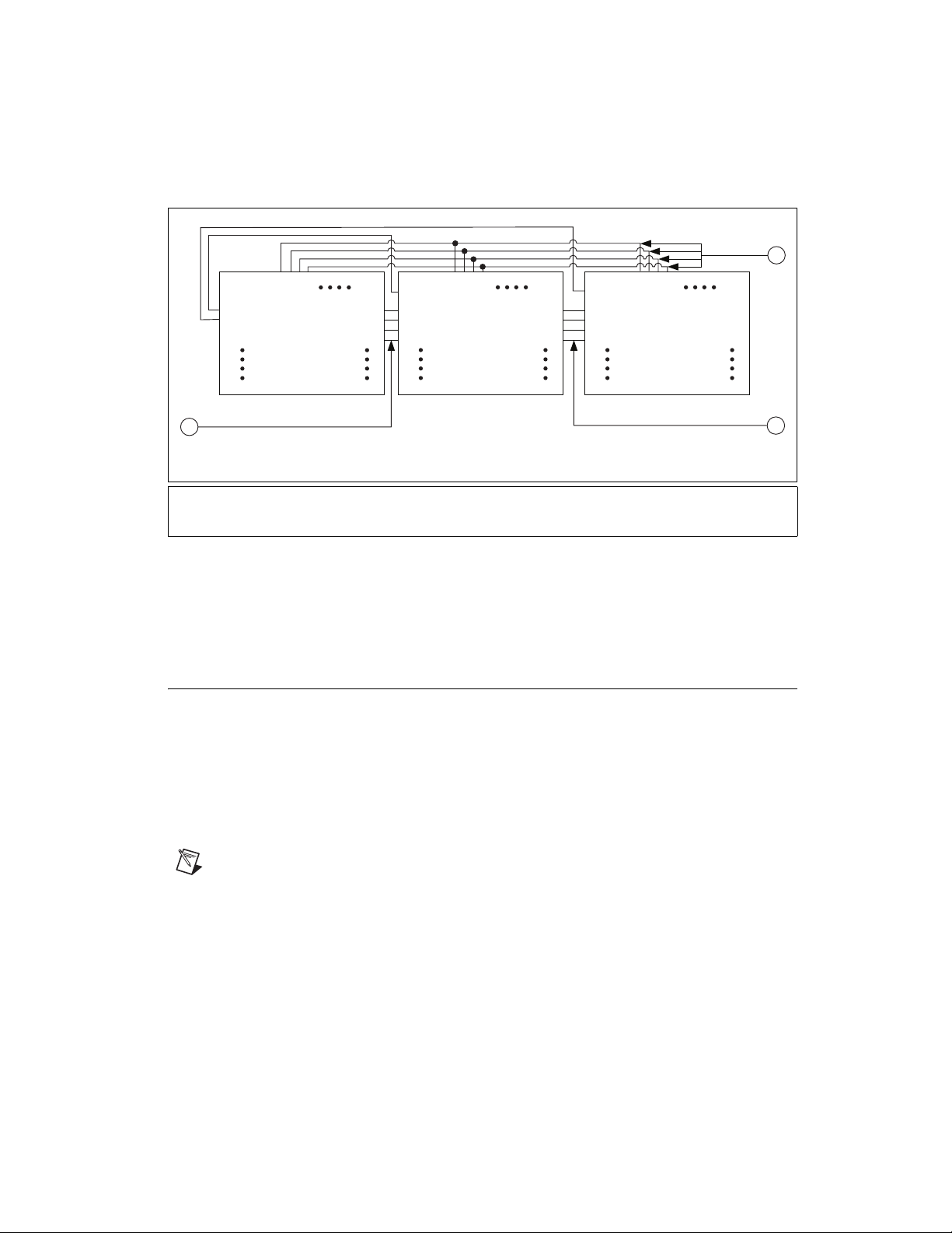
The left local bus lines from the left peripheral slot of a PXI backplane
(Slot 2) are routed to the star trigger lines of up to 13 other peripheral slots
in a two-segment PXI system. This configuration provides a dedicated,
delay-matched trigger signal between the first peripheral slot and the
other peripheral slots for precise trigger timing signals. For example—as
shown in Figure 2-12—an PXI-781x/783x in Slot 2 can send an
independent trigger signal to each device plugged into Slots <3..15> using
the PXI/PXI_Lbl<0..12>. Each device receives its trigger signal on its own
dedicated star trigger line.
Caution Do not configure the NI 781x/783x and another device to drive the same physical
star trigger line simultaneously. Such signal driving can damage the NI 781x/783x and the
other device. NI is not liable for any damage resulting from such signal driving.
Chapter 2 Hardware Overview of the NI 78xx
© National Instruments Corporation 2-23 Multifunction Reconfigurable I/O User Manual
Figure 2-12. PXI Star Trigger Connections in a PXI Chassis
Refer to the PXI Hardware Specification Revision 2.1 and PXI Software
Specification Revision 2.1 at
www.pxisa.org for more information about
PXI triggers.
Switch Settings (NI 781x /783x Only)
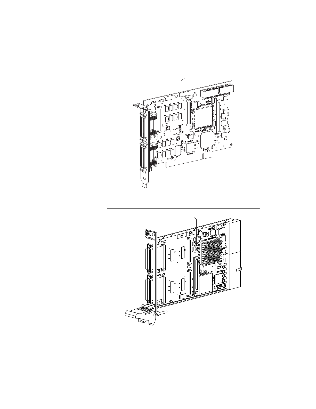
Refer to Figure 2-13 for the location of switches on the PCI-781x and
Figure 2-14 for the location of switches on the PXI-781x. Refer
to Figure 2-15 for the location of switches on the PCI-783x and Figure 2-16
for the location of switches on the PXI-783x. For normal operation, SW1 is
in the OFF position. To prevent a VI stored in Flash memory from loading
to the FPGA at power up, move SW1 to the ON position, as shown in
Figure 2-17.
Note SW2 and SW3 are not connected.
1 Shared Local Bus Lines between Slot 2 and Slot 3
2 Shared Trigger Lines between Slot 2, Slot 3, and Slot 4
3Shared Local Bus Lines between Slot 3 and Slot 4
Lbr0
Lbr1
Lbr2
Lbr3
PXI_Star*
Slot 2
Lbl0
Lbl1
Lbl2
Lbl3
Lbr0
Lbr1
Lbr2
Lbr3
PXI_Star
Slot 3
Lbl0
Lbl1
Lbl2
Lbl3
Lbr0
Lbr1
Lbr2
Lbr3
PXI_Star
Slot 4
3
1
2
* A Slot 2 device ties the PXI_Star Line to the PXI 10 MHz clock
Lbl0
Lbl1
Lbl2
Lbl3
Trigger 0
Trigger 1
Trigger 2
Trigger 3
Trigger 0
Trigger 1
Trigger 2
Trigger 3
Trigger 0
Trigger 1
Trigger 2
Trigger 3
Chapter 2 Hardware Overview of the NI 78xx
Multifunction Reconfigurable I/O User Manual 2-24 ni.com
Figure 2-13. Switch Location on the PCI-781x
Figure 2-14. Switch Location on the PXI-781x
SW1, SW2, SW3
N
I PX
I-
7811R
Reconfigurab
le I/O
CONNECTOR 2 (DIO)CONNECTOR 3 (DIO)
SW1, SW2, SW3