multifunction-rio-user-manual.pdf - 第35页
Chapter 2 Hardware Overview of the NI 78x x © National Instruments Corporation 2-17 Multifunction Reconfigurabl e I/O User Manual Connecting Analog Output Signals The AO signals are AO <0.. n > and AOGND. AO < 0…
Chapter 2 Hardware Overview of the NI 78xx
Multifunction Reconfigurable I/O User Manual 2-16 ni.com
Common-Mode Signal Rejection Considerations
Figure 2-6 and Figure 2-9 show connections for signal sources that
are already referenced to some ground point with respect to the
NI 783x/784x/785x. In these cases, the instrumentation amplifier can reject
any voltage caused by ground potential differences between the signal
source and the device. With differential input connections, the
instrumentation amplifier can reject common-mode noise pickup in the
leads connecting the signal sources to the device. The instrumentation
amplifier can reject common-mode signals when V+
in
and V–
in
(input signals) are both within their specified input ranges. Refer to
the Multifunction Reconfigurable I/O Specifications, available at
ni.com/
docs
, for more information about input ranges.
Analog Output
The bipolar output range of the NI 783x/784x/785x AO channels is fixed at
±10 V. Some applications require that the AO channels power on to known
voltage levels. To set the power-on levels, you can configure the
NI 783x/784x/785x to load and run a VI when the system powers on. The
VI can set the AO channels to the desired voltage levels. The VI interprets
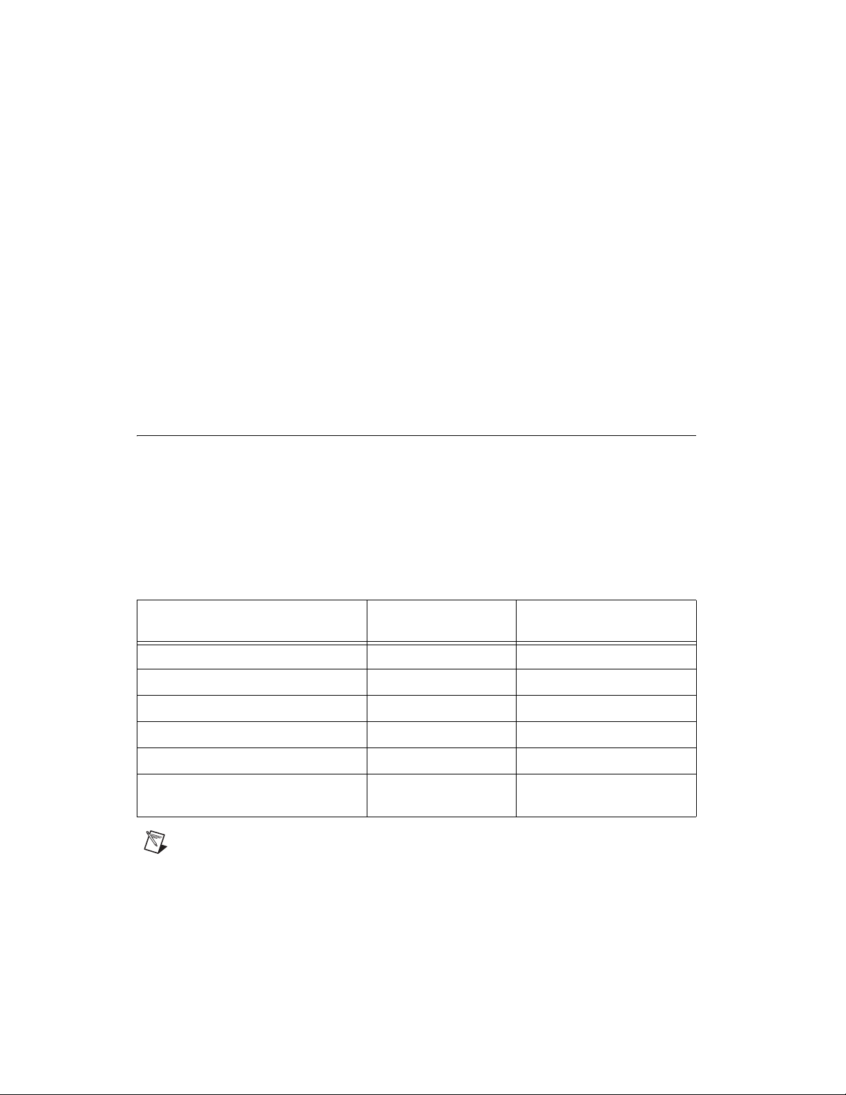
data written to the DAC in two’s complement format. Table 2-3 shows the
ideal AO voltage generated for a given input code.
Note If your VI does not set the output value for an AO channel, then the AO channel
voltage output will be undefined.
Table 2-3. Ideal Output Voltage and Input Code Mapping
Output Description AO Voltage
Input Code (Hex)
(Two’s Complement)
Full-scale range –1 LSB 9.999695 7FFF
Full-scale range –2 LSB 9.999390 7FFE
Midscale 0.000000 0000
Negative full-scale range, +1 LSB –9.999695 8001
Negative full-scale range –10.000000 8000
Any output voltage —
AO Voltage
10.0 V
------------------------------- 32,768×
Chapter 2 Hardware Overview of the NI 78xx
© National Instruments Corporation 2-17 Multifunction Reconfigurable I/O User Manual
Connecting Analog Output Signals
The AO signals are AO <0..n> and AOGND.
AO <0..n> are the AO channels. AOGND is the ground reference signal for
the AO channels.
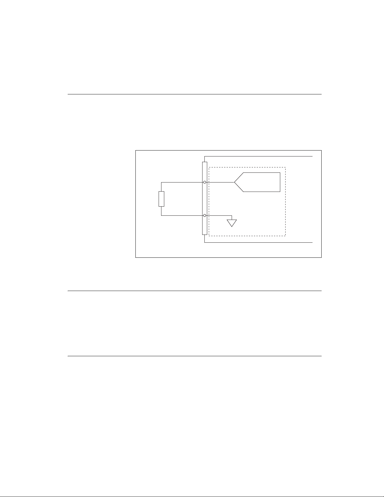
Figure 2-10 shows how to make AO connections to the NI 783x/784x/785x.
Figure 2-10. Analog Output Connections
Digital I/O
You can configure the NI 78xx DIO lines individually for either input or
output. When the system powers on, the DIO lines are at high impedance.
To set another power-on state, you can configure the NI 78xx to load a VI
when the system powers on. The VI can then set the DIO lines to any
power-on state.
Connecting Digital I/O Signals
The DIO signals on the NI 78xx RDIO connectors are DGND and
DIO<0..39>. The DIO signals on the NI 783x/784x/785x RMIO connector
are DGND and DIO<0..15>. The DIO<0..n> signals make up the DIO port
and DGND is the ground reference signal for the DIO port. The NI 781x
has four RDIO connectors for a total of 160 DIO lines. The NI 7830 has one
RMIO and one RDIO connector for a total of 56 DIO lines. The
Load
VOUT 0
+
–
AOGND0
NI 783x/784x/785x
AO0
Channel 0
Chapter 2 Hardware Overview of the NI 78xx
Multifunction Reconfigurable I/O User Manual 2-18 ni.com
NI 7831/7833/784x/785x has one RMIO and two RDIO connectors for a
total of 96 DIO lines.
Refer to Figure A-1, NI 781x Connector Pin Assignments and Locations,
for the connector locations and the I/O connector pin assignments on the
NI 781x. Refer to Figure A-2, NI 783x/784x/785x Connector Pin
Assignments and Locations, for the connector locations and the I/O
connector pin assignments on the NI 783x/784x/785x.
The DIO lines on the NI 78xx support various logic levels. When
configured as inputs, they can receive signals from 5 V TTL, 3.3 V LVTTL,
5 V CMOS, and 3.3 V LVCMOS devices. When configured as outputs, they
can send signals to 5 V TTL, 3.3 V LVTTL, and 3.3 V LVCMOS devices.
Because the digital outputs provide a nominal output swing of 0 to 3.3 V
(3.3 V TTL), the DIO lines cannot drive 5 V CMOS logic levels. To
interface to 5 V CMOS devices, you must provide an external pull-up
resistor to 5 V. This resistor pulls up the 3.3 V digital output from the
NI 78xx to 5 V CMOS logic levels. Refer to the Multifunction
Reconfigurable I/O Specifications, available at
ni.com/docs, for detailed
DIO specifications.
Note 5 V is not supported on all NI 78xx products. See the datasheet & specification of
your product by going to
ni.com/shop/category/multifunction-io.html.
Caution
Exceeding the maximum input voltage ratings, listed in Table A-2, NI 78xx I/O
Signal Summary, can damage the NI 78xx and the computer. NI is not liable for any
damage resulting from such signal connections.
Caution Do not short the DIO lines of the NI 78xx directly to power or to ground. Doing
so can damage the NI 78xx by causing excessive current to flow through the DIO lines.
You can connect multiple NI 78xx digital output lines in parallel to provide
higher current sourcing or sinking capability. If you connect multiple
digital output lines in parallel, your application must drive all of these lines
simultaneously to the same value. If you connect digital lines together and
drive them to different values, excessive current can flow through the DIO
lines and damage the NI 78xx. Refer to the Multifunction Reconfigurable
I/O Specifications, available at
ni.com/docs, for more information about
DIO specifications. Figure 2-11 shows signal connections for three typical
DIO applications.