slau358q.pdf - 第19页
www.ti.com Programming MSP Flash Devices Using the MSP Gang Programmer 19 SLAU358Q – September 2011 – Revised October 2019 Submit Documentation Feedback Copyright © 2011–2019, Texas Instruments Incorporated Operation NOT…

Programming MSP Flash Devices Using the MSP Gang Programmer
www.ti.com
18
SLAU358Q–September 2011–Revised October 2019
Submit Documentation Feedback
Copyright © 2011–2019, Texas Instruments Incorporated
Operation
2.1.1.3 Blank Check
Click the Blank Check button in the Main Dialog GUI to check that the contents of specified memory have
been properly erased. This function is best used after erasing the same segment of memory, using the
button described above. Use the same Memory Options configuration screen shown in Figure 2-2 to
specify which addresses should be erased (Section 2.1.5 describes in detail how to use the memory
configuration window). This function succeeds when the specified memory segments are set to 0xFF, and
fails otherwise.
2.1.1.4 Program
Click the Program button in the Main Dialog GUI to write the contents of a code files to flash memory on
the target device. Addresses specified in the code files are used to determine where the program is
written. Make sure that the regions of memory corresponding to the addresses in the code file are enabled
for writing in the Memory Options configuration screen shown in Figure 2-2 (Section 2.1.5 describes in
detail how to use the memory configuration window).
Configuration conflicts may arise during programming. It is possible that the code the user has chosen is
too big to fit in the flash memory of the target MCU, or the appropriate memory segments have not been
enabled in the Memory Options configuration screen. If this is the case, a warning message appears to
notify the user of insufficient memory; however, the user is still allowed to proceed. If the user proceeds
despite the warning, only the portion of code that fits within the MCU's enabled flash memory is written.
This function succeeds after the programmer has attempted to write code to the specified memory
addresses. Use the Verify function to ensure that the code has been correctly copied to flash on the target
MCU.
2.1.1.5 Verify
Click the Verify button in the Main Dialog GUI to verify that the contents of the target MCU's flash memory
have been properly programmed. This function is best used after programming the same segment of
memory, as performed using the button described above. Make sure that the same memory segments are
enabled in the Memory Options configuration window shown in Figure 2-2, as during programming
described above, to ensure all programmed segments are verified (Section 2.1.5 describes in detail how
to use the memory configuration window).
Verification of selected flash memory is divided into two steps: (1) verify selected flash memory that only
corresponds to the code file, and (2) verify selected flash memory that corresponds to the code file AND
selected flash memory not included in the code file that should be empty (0xFF). Examples of selected
flash memory include Main Memory, All Memory, or User defined, with the exception of Retain Data (if
defined). Verified flash memory that only corresponds to the code file is displayed in the GUI using Verify-
XXXX messages, where XXXX is the start address of a contiguous code segment. Verified flash memory
that corresponds to the code file AND flash memory not included in the code file is displayed in the GUI
using Gl.Verify-XXXX messages; where XXXX is the start address of a contiguous code and empty data
segment. Each contiguous segment is verified using a checksum (CS) and pseudo-signature analysis
(PSA). Verification passes if the CS and PSA match between flash memory and the code file.
If configuration conflicts arose during programming that indicated that the MCU did not contain sufficient
memory for the code to be programmed (either enabled segments or total memory was too small), then
the Verify function verifies only the code that was programmed and ignores the code that could not fit in
memory. This function succeeds if the code in flash matches the code file, and fails otherwise.
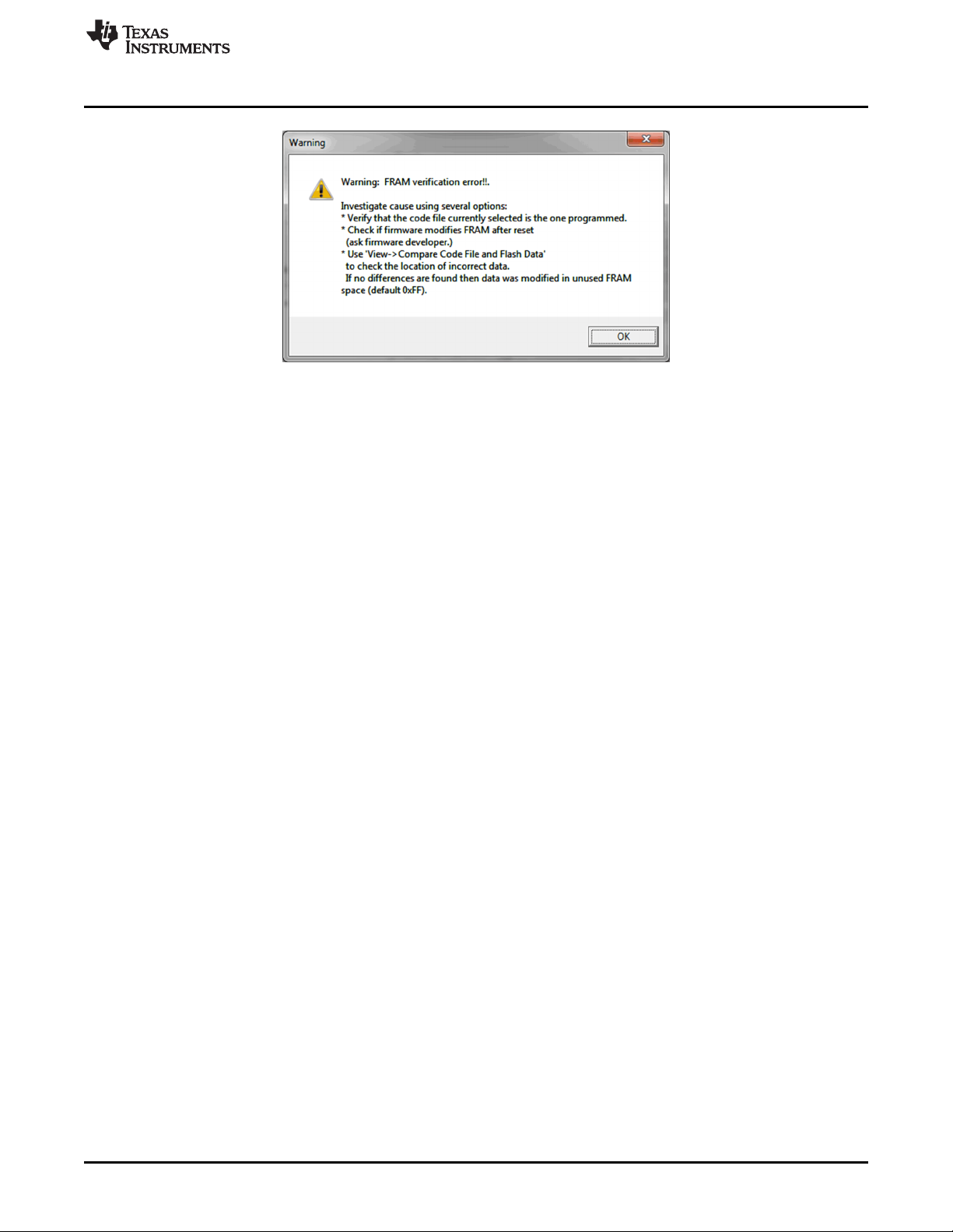
If the verification fails for any reason, TI recommends using an option from the pulldown menu
View→Compare Code File and Flash Data. When this option is enabled, the contents of the Flash or
FRAM memory is read and compared with used code file contents. Only bytes defined in the Code File
contents are compared. All other byte contents taken from the Flash or FRAM are ignored, regardless of
their content. If no errors are found by this verification, even the verification itself failed, then bytes outside
of the code file (not programmed) have a value other than 0xFF. Check the firmware that was downloaded
to Flash or FRAM to determine if the firmware is modifying the Flash or FRAM in unused memory space
after MCU reset (for example, if the Flash or FRAM is used for additional memory space like EEPROM).
If the verification fails and the MCU has FRAM memory, then the following pop-up message is displayed.
www.ti.com
Programming MSP Flash Devices Using the MSP Gang Programmer
19
SLAU358Q–September 2011–Revised October 2019
Submit Documentation Feedback
Copyright © 2011–2019, Texas Instruments Incorporated
Operation
NOTE: Verification failed on MCU with FRAM type memory
Figure 2-4. Verification Error
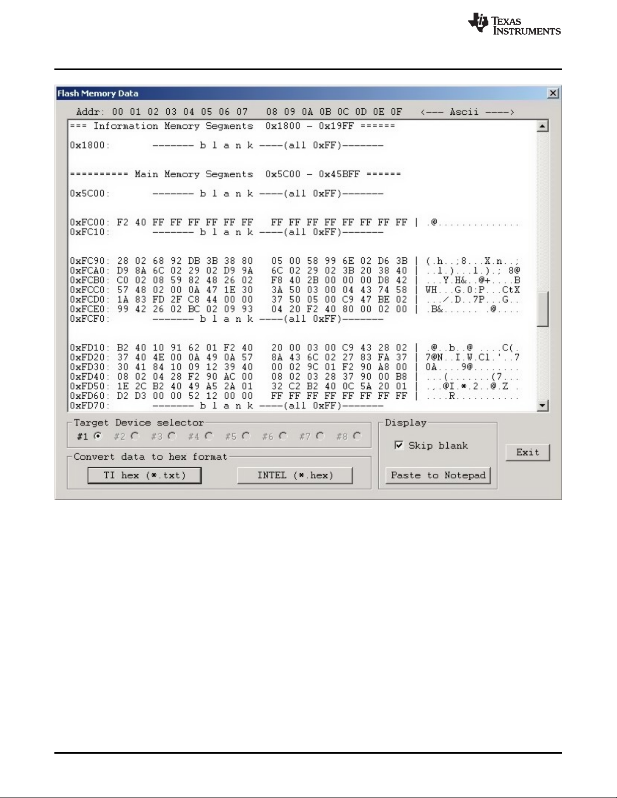
2.1.1.6 Read
Click the Read button in the Main Dialog GUI to read the contents of the target MCU's flash memory. Use
the Memory Options configuration screen shown in Figure 2-2 to specify which addresses should be read
(Section 2.1.5 describes in detail how to use the memory configuration window).
Once used, data is displayed in the Flash Memory Data window as shown in Figure 2-5. This window can
be selected in the View→Flash Memory Data pulldown menu. The Flash Memory Data viewer, shown in
Figure 2-5, displays the code address on the left side, data in hex format in the central column, and the
same data in ASCII format in the right column. The contents of the code viewer can be converted to TI
(*.txt) or Intel (*.hex) file format by clicking on the "TI hex" or "INTEL" button.
Programming MSP Flash Devices Using the MSP Gang Programmer
www.ti.com
20
SLAU358Q–September 2011–Revised October 2019
Submit Documentation Feedback
Copyright © 2011–2019, Texas Instruments Incorporated
Operation
NOTE: This window displays the code addresses on the left side, data in hex format in the center column, and the
same data in ASCII format in the right column.
Figure 2-5. Flash Memory Data
2.1.2 Programming From Image
A programming configuration like the one created in Section 2.1.1 can be stored in the form of an image.
The advantage of an image is that it contains both the configuration options necessary for programming
as well as the code files that are flashed to target devices. Moreover, only images can be saved to internal
MSP Gang Programmer memory and used in Standalone mode, in which the programmer can operate
without being connected to a PC. Using the From Image mode allows the user to test images with full GUI
support before committing them to production.
When an image has been created, it can be used to greatly simplify programming by using the procedure
described in Section 2.1.9. Figure 2-6 shows the main dialog GUI where the From Image option is
selected for programming (top left corner). Here the user can load an image from MSP Gang Programmer
internal memory. An image can be created in Interactive Mode and saved to the programmer. One of 96
different images can be selected from internal memory, or one image from each external SD-Card can be
used.