slau358q.pdf - 第36页
Programming MSP Flash Devices Using the MSP Gang Programmer www.ti.com 36 SLAU358Q – September 2011 – Revised October 2019 Submit Documentation Feedback Copyright © 2011–2019, Texas Instruments Incorporated Operation NOT…
www.ti.com
Programming MSP Flash Devices Using the MSP Gang Programmer
35
SLAU358Q–September 2011–Revised October 2019
Submit Documentation Feedback
Copyright © 2011–2019, Texas Instruments Incorporated
Operation
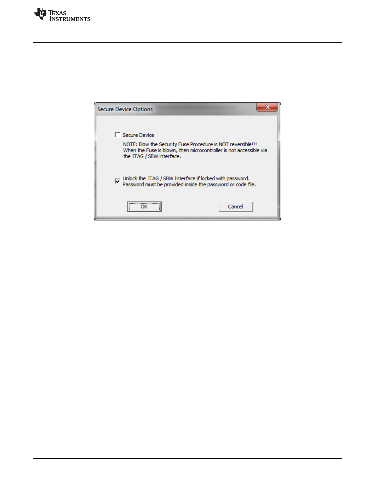
2.1.6 Secure Device Setup and Memory Protection
The MSP430 family has an option to block access to the MCU through the JTAG and SBW interface. To
select the Secure Device option, press the Secure Device Option button on the GUI or select the option
from the pulldown menu under Setup→Secure Device. Figure 2-13 shows the Secure Device Options
window. When the Secure Device option is selected, the device is secured at the end of the GO
programming procedure if all programming steps pass successfully. Otherwise, the device is not secured.
For MSP430 devices, the Secure Device process is not reversible.
NOTE: Irreversible unless password option used. Can be done automatically after programming (at end of GO
operation)
Figure 2-13. MSP430 Secure Device Options
In some MCUs, typically the FRAM family, a lower JTAG and SBW protection level is available. The JTAG
and SBW can be protected by password that is saved in the MCU flash at the addresses 0xFF80 through
0xFFFF. If the password in the code file at this address is the same as the password saved inside the
flash, then access to JTAG and SBW is unlocked, and flash can be reprogrammed. This is useful for
updating firmware after initial programming.
However, if the device is secured using the Secure Device procedure, then unlocking by using this
password is no longer possible. The Secure Device mechanism provides a higher level of protection.
The MSP432 family implements a different approach to memory protection. The MSP432 can provide
protection for selected memory regions or to block communication. All protection options are described in
the MSP432 technical reference manual and are implemented by programming the flash mailbox (see the
MSP432P4xx Family Technical Reference Manual (SLAU356) for details). The MSP-GANG can program
the flash mailbox according to user settings or directly from a code file. When the Secure Device Option
button is selected for the MSP432 family, the Secure Device Options screen is displayed (see Figure 2-
14).
Programming MSP Flash Devices Using the MSP Gang Programmer
www.ti.com
36
SLAU358Q–September 2011–Revised October 2019
Submit Documentation Feedback
Copyright © 2011–2019, Texas Instruments Incorporated
Operation
NOTE: The flash mailbox can be programmed to provide memory protection of some memory, or communication
can be blocked. Can be done automatically after programming (at end of GO operation)
Figure 2-14. MSP432 Secure Device Options
www.ti.com
Programming MSP Flash Devices Using the MSP Gang Programmer
37
SLAU358Q–September 2011–Revised October 2019
Submit Documentation Feedback
Copyright © 2011–2019, Texas Instruments Incorporated
Operation
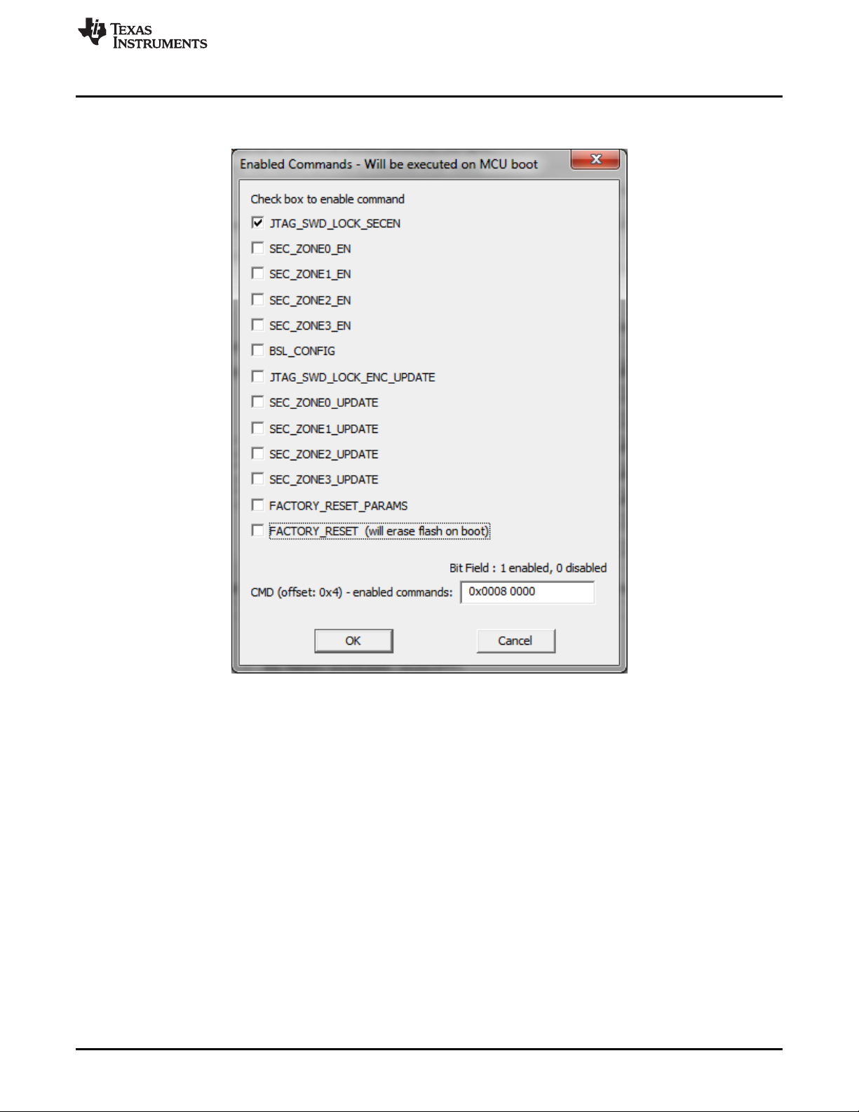
Many types of protection options are available and can be set in the Enabled Commands screen (see
Figure 2-15).
NOTE: The flash mailbox can be programmed with different instructions that provide memory protection, or block
communication.
Figure 2-15. MSP432 Secure Device Options Details
2.1.7 Programming MCU With IP Encapsulated Segment
Some FRAM MCUs have the option to protect an address range in main memory. All data from protected
memory space is read as 0x3FFF regardless of actual contents. When the protected memory is not
locked, then the contents can be read "as is" if the option "Including Unlocked MPU-IPE" is selected. The
programmer must have the address range of protected memory to be able to service the MCU correctly.
The protected memory range must be specified in the MPU-IPE Space Addresses Group in the Memory
Options window (see Figure 2-16). The protected memory space can be erased and reprogrammed when
the option "Including Locked or Unlocked MPU-IPE space" is selected. That option can only be selected
when the All Memory option is selected. When the memory region is protected and locked using the MPU-
IPE features (see MCU family user guide or technical reference manual for details) then all memory is
erased first before programming the MCU. The protected and locked MPU-IPE memory range can be
erased and reprogrammed only when the JTAG or SBW communication is used. When BSL
communication is used, the locked memory cannot be erased or reprogrammed. Through BSL, memory
can only be erased and reprogrammed when the locking option is not used.