PPS Pro version 8.2.pdf - 第120页
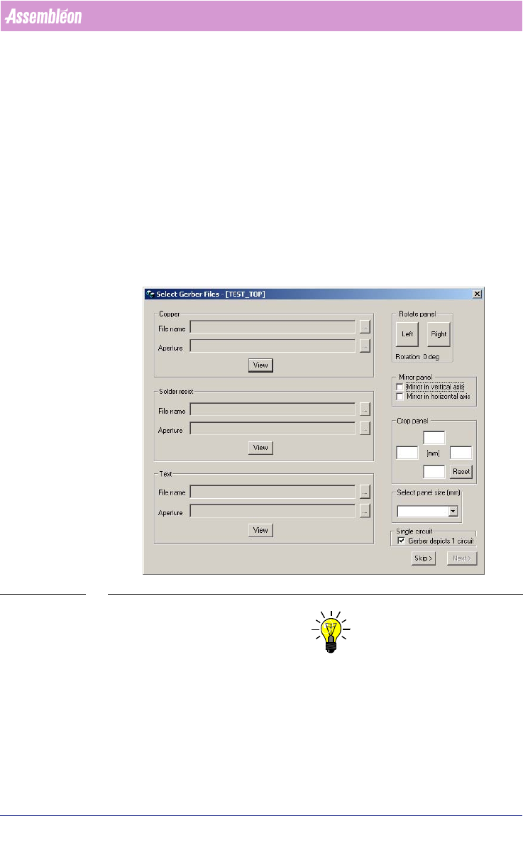
User Manual 4022 591 98247 116 PPS-Pro v8.2 05.07 Guidelines for using PPS-Pro 3.3.4.2 “Select Gerber Files” Window For t hre e d i ff ere nt l a yers in fo rm at io n ca n b e adde d to m ake s ure co rre ct artwork is …

4022 591 98247 User Manual
05.07 PPS-Pro v8.2 115
Guidelines for using PPS-Pro
//Position Shape XYR DCODE SHAPE
1 LINE 100.0 D70
2 LINE 125.0 D71
3 LINE 150.0 D20
4 CIRCLE 20.0 D21
5 CIRCLE 43.0 D22
6 RECTANGLE 43.5 43.5 0 D26
7 CIRCLE 91.0 D27
8 CIRCLE 118.0 D28
9 CIRCLE 67.0 D30
FIGURE 10 Example as starting aperture file
In the correct Aperture file see FIGURE 11 "A correct Aperture file for artwork
extraction" on page 115 all comments are removed. The first line contains the
unit-size for all X / Y Columns. Notice that several apertures have only one
dimension (‘CIRCLE’ and ‘LINE’). So extra values (dimension) must be added for
these shapes. Also notice that the columns are comma separated.
UNIT,=,MILS
70,LINE,100.0,0
71,LINE,125.0,0
20,LINE,180.0,0
21,CIRCLE,20.0,0
22,CIRCLE,43.0,0
26,RECTANGLE,43.5,43.5
27,CIRCLE,91.0,0
28,CIRCLE,118.0,0
30,CIRCLE,67.0,0
FIGURE 11 A correct Aperture file for artwork extraction
3.3.4 Artwork extraction
3.3.4.1 Select gerber files for artwork extraction
Step one from the pre optimizing stage for Local mode is the collection of files
needed for artwork extraction. Gerber files and aperture files need to be
selected. Make sure the files have correct formats
(see 3.3.3.6 "Preparing the
Gerber files" on page 112) and select all appropriate files. When the calcu-
lation is started (Optimize Cell) a gerber files selection window is presented,
which is described in the following paregraph.
User Manual 4022 591 98247
116 PPS-Pro v8.2 05.07
Guidelines for using PPS-Pro
3.3.4.2 “Select Gerber Files” Window
For three different layers information can be added to make sure correct
artwork is used for the fiducials:
a) Copper: This is the layer that represent the copper layer of the
PCB.
(see SCREEN 67 on page 116)
b) Solder resist: This layer represent the solder resist layer (in
most cases this is a green semi transparent layer) or the solder
layer. In most cases this layer is solder paste that is printed on
the PCB and therefore cannot be used for artwork/fiducials.
c) Text: This layer represents the text that can be printed over the
other layers. In most cases this layer is printed text that
cannot be used for artwork/fiducials.
SCREEN 67 Select Gerber Files Window
NOTE: “Text”-layers is optional. This means that if this layers is not used or not
present it can be skipped. In some cases it has been observed that some
artwork could not be recognised in combination with text layers.
1. “File name”: The appropriate gerber file that is used for that specific layer
Copper, Solder resist or text.

4022 591 98247 User Manual
05.07 PPS-Pro v8.2 117
Guidelines for using PPS-Pro
2. “Aperture”-File: Select appropriate aperture file that comes with the
Gerber data and that has the correct layout.
(see n "Creating the correct
aperture file" on page 113)
3. “View”-button: For each of the Layers in the Gerber data a “View”-button
is present that can be used to check what the result is for that specific
layer combination of gerber file and aperture file.
(see 3.3.4.3 "“PCB
Artwork” Window" on page 118)
4. “Rotation panel”-buttons: If the artwork is not shown correctly in the PCB
artwork window the artwork can be rotated to the Left or to the Right by
pushing these buttons. To see the artwork again the “View”-button must
be used to see the results. The rotation is done for all tree layers.
5. “Mirror panel”-frame: If the artwork is not shown correctly in the PCB
artwork window, the artwork can be mirrored by using the selections
“Mirror in vertical axis”, “Mirror in horizontal axis”.
6. “Crop panel”-frame: 4 sizes can be entered that define a panel size. By
entering these the artwork becomes smaller. The Artwork is cropped. By
using the “View”-button the results can be seen in the “PCB artwork”
window.
(see 3.3.4.3 "“PCB Artwork” Window" on page 118).
7. “Select panel size (mm)”-frame: After selecting the correct gerber and
aperture file a possible board size are calculated. In most cases the correct
panel size is selected but can be changed by using this ComboBox.
8. “Skip”-Button: If you can have products which are quite small (or a panel
with several boards) and these panel have several fiducials. These products
you can already optimize in LOCAL mode without having to use the
artwork extraction.
9. Single Circuit: In sole cases gerber files will be provided that represent one
circuit (board) of a multi-circuit PCB, enable this option to automatically
create the required number of circuits. If the gerber files visualize the
complete board, then disable this option.
NOTE: This means that over the PCB there must be enough fiducial so always 2
fiducials with a maximum difference in X direction of 75 mm are available.
If this is not the case an error is created and the option “Continue”-Button
must be used meaning that artwork extraction (Gerber) must be done.
10. “Next”-Button: After the PCB Artwork window shows the correct graphical
presentation of the files this button can be selected and the artwork
extraction continues with the next step.
(see 3.3.4.4 "Aligning artwork
with Cad-data" on page 118)