PPS Pro version 8.2.pdf - 第50页
User Manual 4022 591 98247 46 PPS-Pro v8.2 05.07 PPS-Pr o GUI 3. Select one o f the presented types: Cente rRad ius i s a n ormal cir cuit, th e remain der of this e xampl e uses this typ e . 4. En ter th e (X, Y) coor d…
4022 591 98247 User Manual
05.07 PPS-Pro v8.2 45
PPS-Pro GUI
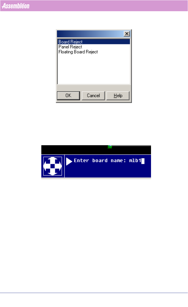
Board Rejects relate to circuits
Panel Rejects relate to PCBs or to Areas (A-Series)
Floating Board Rejects relate to circuits, but can have different locations than
the circuits themselves.
4. Complete the data entry, example for a board badmark:
5. Enter the location (X, Y) coordinates, or click on the location in the PCB
where the badmark should occur.
6. When the requested badmark(s) is/are present press enter to complete this
data entry.
Note that board rejects relate to a board (=circuit) these are copied along with
the circuits.
2.13.6 Entering reference holes
After CAD import information about reference holes is not always present,
this can be important for FCM and FCM Multiflex machines. The optimizer for
these machines requires one or 2 (Multiflex) reference holes to be defined.
These can be entered as follows:
1. Start MDF edit on the imported PCB.
2. Select Add > Circle
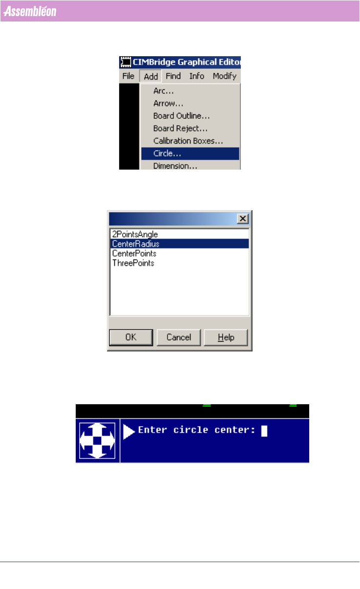
User Manual 4022 591 98247
46 PPS-Pro v8.2 05.07
PPS-Pro GUI
3. Select one of the presented types:
CenterRadius is a normal circuit, the remainder of this example uses this type.
4. Enter the (X, Y) coordinates of the circle center:
5. Enter the radius of the circle.
6. Steps 4 and 5 can be repeated until all circles have been entered.
7. Finally press enter (as circle center) to complete the data entry.
To turn a circle into a reference hole proceed as follows:
4022 591 98247 User Manual
05.07 PPS-Pro v8.2 47
PPS-Pro GUI
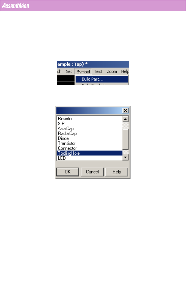
1. Take care that no other item is selected (use ctrl-d to ensure this) Click on
one circle in the MDF editor (it is not correct to select all circles since that
would turn them into one object). The circle is now the only purple object
shown.
2. Select Symbol > Build Part
3. Select ToolingHole from the selection list:
4. Click on the next circle and repeat step 3 until all (required) circles have
been turned into ToolingHoles.
2.14 Fiducial arrangements and Badmark Grouping
As the number of circuits on a PCB increases, the number of fiducial meas-
urements and (possible) badmark sensing activities performed by a Camera
also increases. In some cases the time that is needed by the Camera will
dominate the cycle time of the entire machine, which is not desirable. To
avoid this domination the concepts of fiducial arrangements
(see 2.15 on page
48) and badmark groupings (PowerLine) (see 2.16 on page 48) or area
badmarks can be used.
Fiducial arrangements enable the usage of the same set of fiducials for
multiple circuits.