F5HM Circuit Diagrams.pdf - 第138页
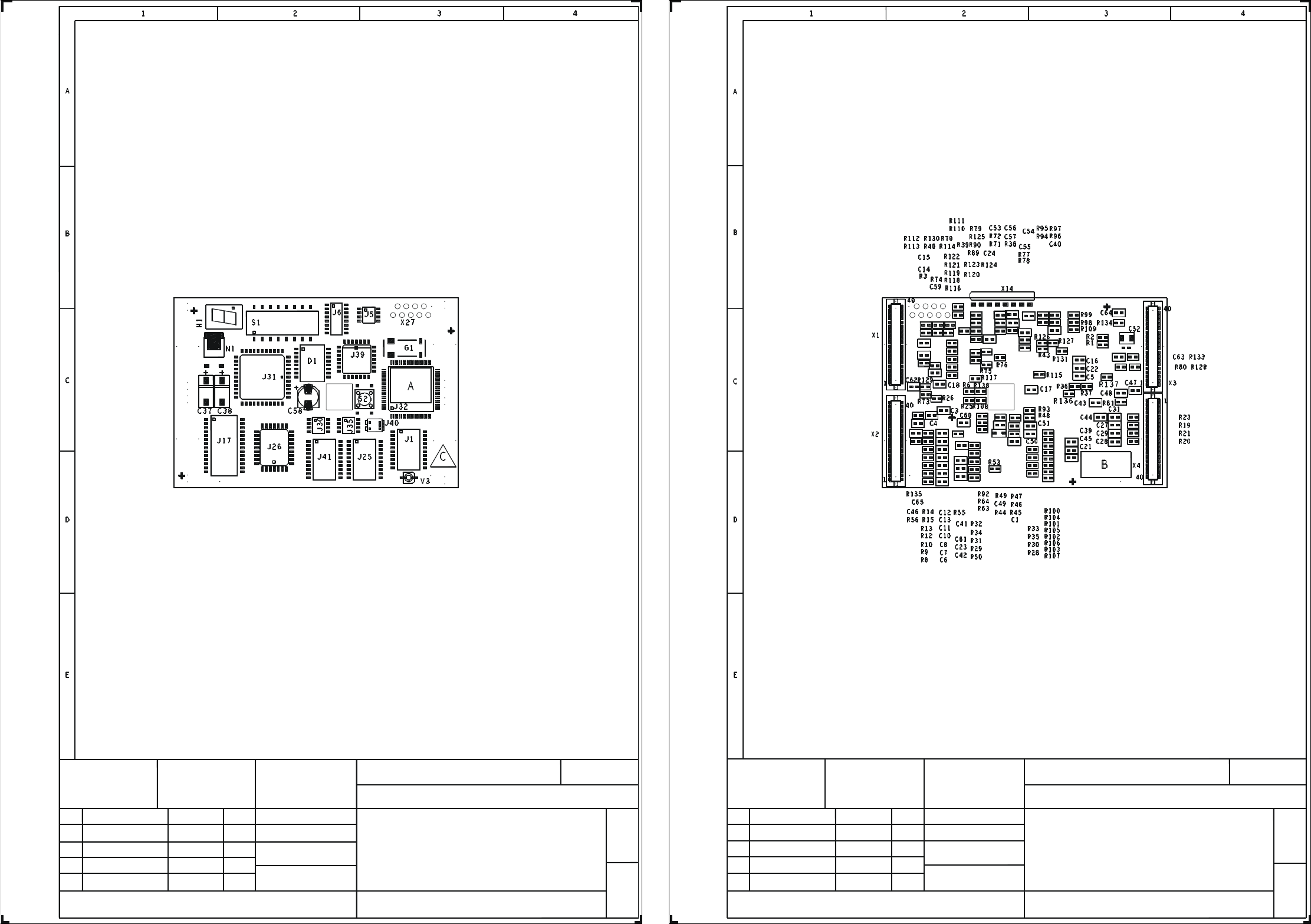
4 Printed Circui t Boards 138 0034390 8-010101 ND4 856 PCB , servo ba ckplane, S 23 (Sh. 1 of 2) 0034390 8-010101 ND4 856 PCB , servo ba ckplane, S 23 (Sh. of 2) Compon ent di agram, co mpone nt si de 856 p rintec c ircu…
4 Printed Circuit Boards 137
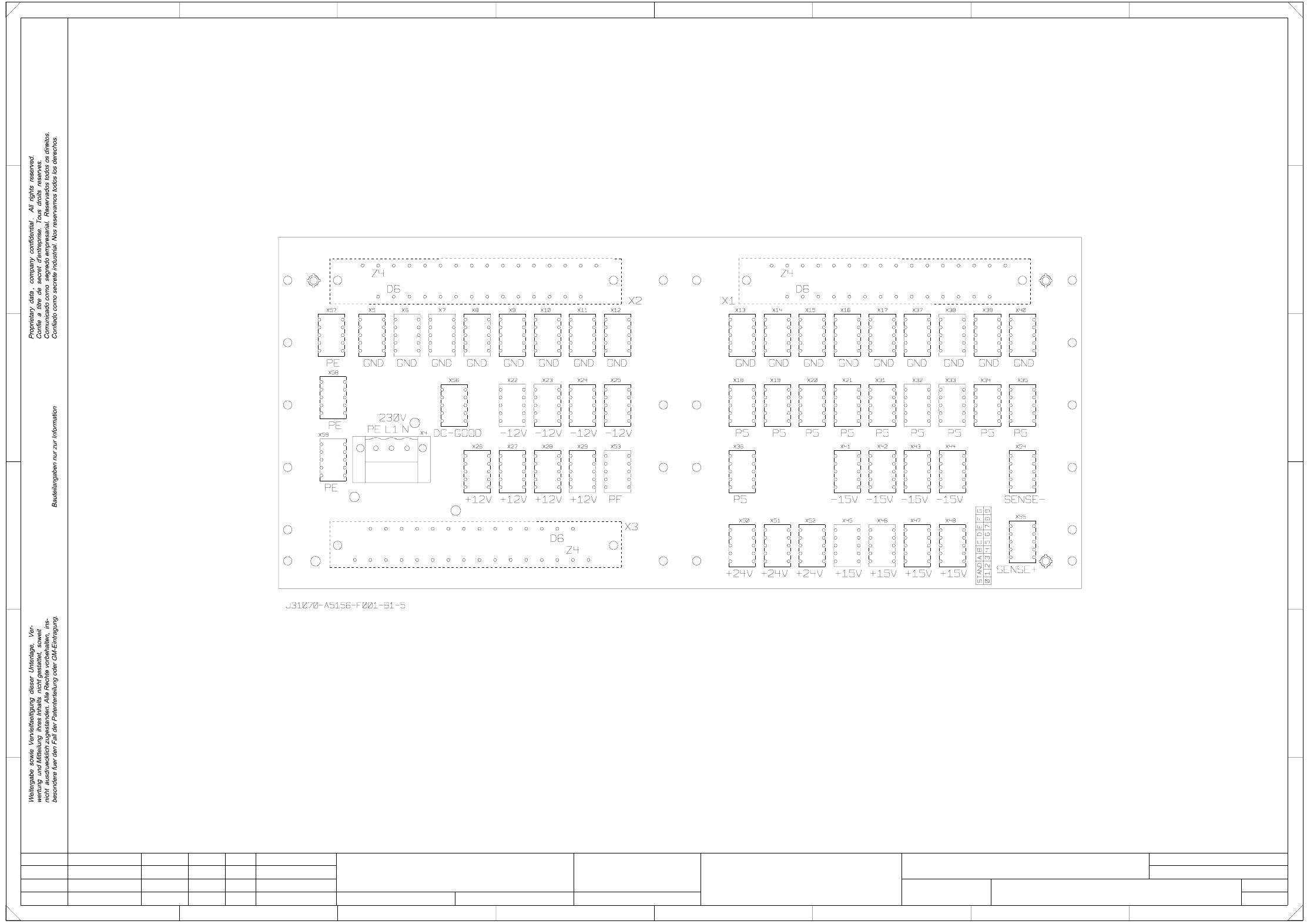
00342582-020101ND3 S23 backplane
1
1
S23 backplane
wired component side 1
5156/2
b) space for inspection label
a) space for identification label
=
Datum
Gepr.
Norm
Bearb.
Sheet
Urspr. Ers. f. Ers. d.NameDatumAenderungZustand
SIEMENS AG
Sh.
+
C
765432
A
1
E
F F
E
D
B
2
B
8
D
1
A
C
8765
B1 Kg
34
00342582-020101ND3
Component diagram
#
Krieg
08.10.98
08.10.98
4 Printed Circuit Boards 138
00343908-010101ND4 856 PCB, servo backplane, S23 (Sh. 1 of 2)
00343908-010101ND4 856 PCB, servo backplane, S23 (Sh. of 2)
Component diagram, component side
856 printec circuit board
S23 servo backplane
G32918-K0086-B001-*-17
00343908-010101ND4
Sheet
1+
SIEMENS AG
ANL TD E E
FETTICH
04.03.98Datum
Name
FE
NameDatum
04.03.98
MitteilungZust.
51
52
05.10.98 KL
Component diagram, solder side
856 printed circuit board
S23 servo backplane
G32918-K0086-B001-*-17
00343908-010101ND4
Sheet
2-
ANL TD E E
SIEMENS AG
FETTICHName
Datum 04.03.98
KL
FE
NameDatum
04.03.98
05.10.98
MitteilungZust.
51
52
DVL Lage Unterlage Zustand
1 234 5
X = Pinch off pin 5 from plug X3
A = Identification label
B = Inspection label
- - - - - -
- - - - - -
4 Printed Circuit Boards 139
00344485-010101ND4 877 PCB, processor board 80C515C (Sh. 1 of 2)
00344485-010101ND4 877 PCB, processor board 80C515C (Sh. 2 of 2)
ESD label
Inspection label on solder side
Identification label on J32
- - - - - - -
- - - - - - -
- - - - - - -
MITTEILUNG
ZUST.
01
03
02
DATUM
07.12.98
NAME
KL
06.07.00
03.01.99
KL
KL
A
C
B
G32918-K0113-B001-*-0017
00344485-010101ND4
8-layer PCB
80C515C
Processor board
Mounting diagram, component side
ATD TD MCH 2
SIEMENS AG
NAME
DATUM
Klose
07.12.98
PCB 877
M 1 : 1
1 +
Sheet
- - - - - - -
- - - - - - -
- - - - - - -
MITTEILUNG
ZUST.
01
03
02
DATUM
07.12.9
8
N
A
M
E
K
L
06.07.0
0
03.01.9
9
K
L
K
L
G
3
2
9
18-K0113-B001-*-0017
0
0
3
4
4485-010101ND4
8
-
l
a
y
e
r
PCB
8
0
C
5
15C
P
r
o
c
e
ssor board
M
o
u
n
t
i
n
g
dia
g
ram, component side
A
T
D
T
D
M
C
H
2
S
I
E
M
E
N
S
A
G
N
A
M
E
D
A
T
U
M
K
l
o
s
e
0
7
.
1
2
.
9
8
P
C
B
877
M
1
:
1
2 -
Sheet