F5HM Circuit Diagrams.pdf - 第59页
2 Circuit Diagr ams 59 0033681 2-020102 LD3 Power su pply circu it diagram ( Sh. 2 of 2) 1.0mm ² 1.0mm ² 1.0mm ² 1.0mm ² 2 2 SMD-Placement System Siplace S23 Prod uct status Doc. sta tus Funct ion s tatus = Datum Gepr. N…
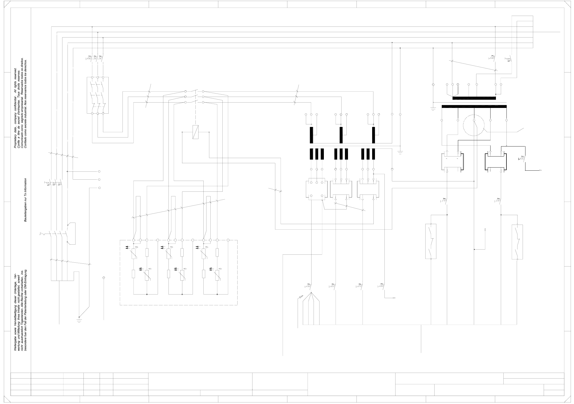
2 Circuit Diagrams 58
00336812-020102LD3 Power supply circuit diagram (Sh. 1 of 2)
10A
4
~~
-
V3
105
105
105
11
12
1L+
1L+
F4
20A
+
~
2
3
5
00324356-xx
K2
7
8
9
10
00300161-06
F8
1
14
2L-
6
7L+
K2
GND
13
F9
10A
2
1
2
10A
B
4L+
5L+
1
2
24V AC
24
40A
+
10A-
34
~~
~~~
13
62
8
PE
16A
PE
F2
3313 23
6
12
48
1L-
13 14 16
48
15
42
42
42
17 18
400
23
0V
19
10A
2
400
208
83
9
V4
+36A
N
PE
7
24
Q1
16A
10A
L3L1 L2 N
T3T1 T2 N’
2414
F10
T2
K1
400
4
5
8
0
11
24
+5%
120
150
4 5
230
230
6
24
48
13
N
X200
3
8
208
400
208
400
7152
400
-5%
PE
F1
1 2
--
~
V5
+
36A
~
6A
2
1
T1
10 9
6
6A
5
F11
1
1
F3
10A
bk
2
N
2
1
2
SMD-Placement System Siplace S23
Product status
Doc. status
Function status
(move wire 3 from terminal 13 to terminal 14
connected in parallel, if the machine is
continue systematically for the other phases)
The inrush current limiter has to be
move wire 2 from terminal 12 to 13
operated at 120V
Jumper is part of the main switch.
Remove jumper if nessecary (IT power
supply) (France, Italy, Japan, U.S.A.)
bk
2,5mm²
2,5
bk
bk
2,5mm²
bk
bk
bk
bk
bk
(Lifting table)
(dp1/Z axes)
bk
per sleeve
gr
rd
bl
bk
4
bk
bk
bk
bl
gnye
gnye
bl
cover for
supply
power
base
To
Power
main power
To
filter 1
gnye
Two wires
2
(Star/lifting table)
(Tape cutter)
C0508-W1 gr
external emergency stop
To sheet 2
2,5mm²
bk
1,5mm²
bk
1,0mm²
To
sheet 2
bk
bk
(Star, slow)
2,5mm²
bk
(X,Y slow)
bk
To sheet 2
1,0mm²
bk
wh
gnye
br
bk
V3(-)
2L-(0V)
2
6
1
3
5
Inrush current limiter
11 12 13
wh
bk
supply
gnye
bl
gnye
4
3
bk
1
switch
Main
2,5mm²
2.5mm²
double-ended ferrule
bk
bk
1,5mm²
mm²
2,5mm²
bk
3
4
5
7
8
9
22
bk
14 21
br
23 24 31 32 33 34
2,5mm²
bk
bk
bk
Join strands
in a
bk
4,0mm²
bk
bk
bk
bk
10,0mm²
terminal panel,
righthand side
2,5mm²
bk
2,5mm²
A1
00342917-XX (W3)
00342917-XX (W1)
gnye
2,5mm²
1,5mm²
Attention !
6
1
2
~
righthand side
terminal panel,
To
To
bk
terminal panel,
To
(X,Y axes)
bk
bk
bk
bk
bk
bk
bk
righthand side
F
E
D
C
B
A
8
A
00341193-xx
00324358-xx
V1
Power supply circuit diagram
24V AC
1
1L+
10
25R
56R
25R
56R
56R
25R
56R
25R
56R
25R
A2(-)
56R
25R
PL EA1 E
K4
A1(+)
=
Datum
Gepr.
Norm
Bearb.
Blatt
Urspr. Ers. f. Ers. d.NameDatumAenderungZustand
SIEMENS AG
Bl.
+
00336812-020102LD3
Leh
Leh
Deu
02
01
02
02.09.98
23.01.98
04.12.98
04.12.98
Werner
#
C
D
E
F
1L+
2L+
3L+
bk
6L+
1
F5
2
10A
2
F6
1
F7
11
4
PE
6
78
1234567
1
3456
V2
-+
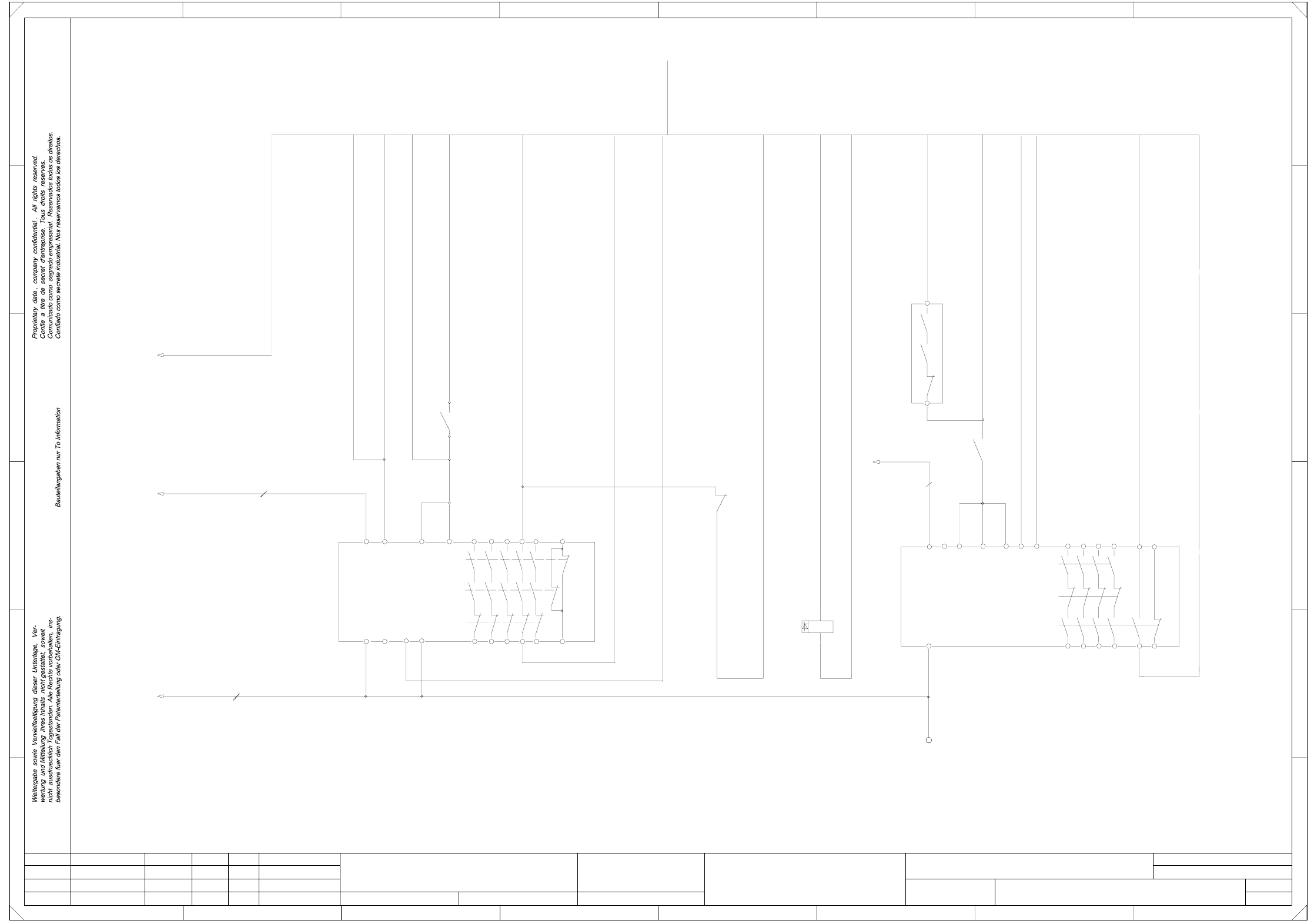
2 Circuit Diagrams 59
00336812-020102LD3 Power supply circuit diagram (Sh. 2 of 2)
1.0mm²
1.0mm²
1.0mm²
1.0mm²
2
2
SMD-Placement System Siplace S23
Product status
Doc. status
Function status
=
Datum
Gepr.
Norm
Bearb.
Blatt
Urspr. Ers. f. Ers. d.NameDatumAenderungZustand
SIEMENS AG
Bl.
+
PL EA1 E
X3 X5X4 X6
12345678
12
F
E
D
C
B
A
GND
K1
5343
3323
X2
X6
X4 24
14 544434
66
3TK2805
24V AC
L2
3TK2804
A1
K2
L1 X1 X2
66
24V AC
K3
14
13
21
24V AC
+24V DC
00321113-xx
lefthand side
345678
A
B
C
D
E
F
6557433323
13
13
L1 X1 X3 X5
65
22
K3
K3
MP1
A2
L2
3414
24
44 58
24V AC
F10:2
54
44
K3
43
K1
53
+24V DC
To sheet 1
gr/bn
ye
terminal panel
To
From On push-button
wh/gr
rs
gr/pk
bk
vi
rd/bl
ye/bn
wh/ye
To S5 input X2kd:1
From On push-button
wh
gn
br
bl
wh/gn
bn/gn
Software release signal
Signaling circuit
Software release signal
gr
To S5 input X2kd:8
Control On
Signaling circuit
From EMERGENCY STOP circuit (to K1)
To On push-button
To ext. EMERGENCY STOP circuit (WPW)
To sheet 1 F7:2
24V AC switched
bk
To sheet 1 F10:2
bk
To sheet 1
Leh
Leh
Deu
02
01
02
02.09.98
23.01.98
04.12.98
04.12.98
Werner
#
Power supply circuit diagram
00336812-020102LD3
To On push-button
To key-operated switch
(to K2)
From EMERGENCY STOP circuit
To GND S5 Baugruppe X2kc:M
To S5 output X2kc:8
To S5 input X2kb:7
Software release signal
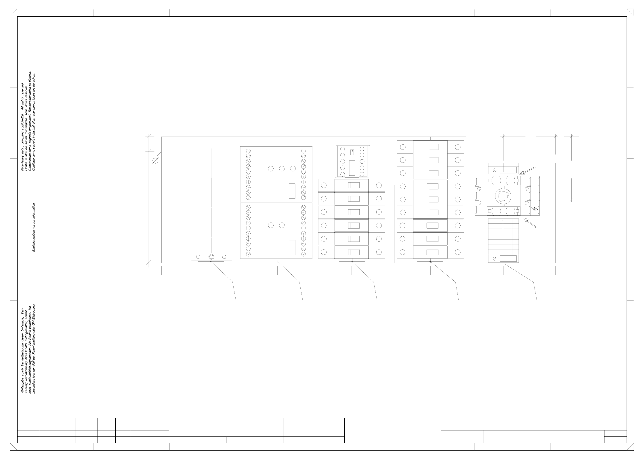
2 Circuit Diagrams 60
00336812-020102TD3 Power supply structure (Sh. 1 of 4)
F11
57
1
4333
F10
10A
20A
54
K1
34
13 23X5
1
10A
0
F9
2
10A
170.0
66
MP1
0
2
16A
0
F2
4
4
1
0
5
0
2
1
0
2
0
2
1
0
2
l=130mm
535.0
470.0
14 24X6
F4
PE
l=146mm
l=160mm
66
0
1
F1
24
85.0
NNN
5
N
Q1
31
X1 X3
1
L1
2
F8
l=146mm
l=164mm
0.0
167.0
73.0
10A 10A
1
5834 44
K2
F6
65
K3
0
3
10A
2
1
X200
2
6
0.0 21.2
6.0
Channel 1
PE PEPE
N
14X6X2 X4 X2 X4L244
4
2
65.0
0
F3
10A
2
1
0
0
5
6
6
X1 X3 X5
F7
0
2
1
53
F5
Channel 2
Power
L2
16A
3
0
On
Ready
L1
13 23 33 43
This lateral freedom of movement is needed to achieve optimum passage through the front panel.
It must be possible to move the main switch up to 2mm to the left/right on the top-hat rail.
The X200 terminals on the upper top-hat rail must be seated flush on the right, against the stop.
Note!
1234567
FF
E
C
B
A
TS35 - Top-hat rail
TS35 - Top-hat rail
TS35 - Top-hat rail
TS35 - Top-hat rail
TS35 - Top-hat rail
678
A
8
12345
B
C
D
E
Leh
Leh
Deu
02
01
02
02.09.98
23.01.98
04.12.98
04.12.98
Werner
#
Power supply structure
00336812-020102TD3
D
=
Datum
Gepr.
Norm
Bearb.
Blatt
Urspr. Ers. f. Ers. d.NameDatumAenderungZustand
SIEMENS AG
Bl.
+
PL EA1 E
270.0
370.0
65
6A
1
4
SMD-Placement System Siplace S23
Product status
Doc. status
Function status