F5HM Circuit Diagrams.pdf - 第57页
2 Circuit Diagr ams 57 0033681 2-020101 FD3 Safety conce pt, overview ( signaling circuit) (Sh. 3 of 3) 3 3 SMD-Placement System Siplace S23 Product statu s Doc. statu s Fun ction status (Signaling circuit) = Dat um Gepr…
2 Circuit Diagrams 56
00336812-020101FD3 Safety concept, overview, safety circuit (Sh. 2 of 3)
machine ON
release signal for
(Input)
(ON button)
Key-operated switch
Safety circuit
Emergency stop mushroom-head push-button
(output)
Emergency stop mushroom-head push-button
5678
12
FF
E
D
C
B
A
(input)
safety loops
Connection for external
Cover switch
1234
13
X6
24V AC
24
14 34 44 58 66
L1
K2 3TK2804-0AC2
K3’
K2’
H2’
K3’
K1’ K3’
K1’
K2’
3323
K1 3TK2805-0AC2
K1’
K2’
H1
K3’
K2’K2’
K1’ K3’
L2
K1’ K2’
X1
(1-n)
Y0413-S1
X211
X211
Y0906-S1
Y0907-S1
~24VAC
H1’
3414 24
K1’
L1 X1
K1’
5743
44
E
78
A
B
C
D
K3’
K1’ K2’
H2
H3
K1’
K2’
13
X5
X3
24V AC
X6
L2
C0952-K3
Y0438-S1
K3’
65
Y0906-S2
Y0907-S2
C0952-K3
44
54
66
X4
K1’
K2’
K3’
X5
K3’
X3
43
54
53
Y0907-S4
K1
65
X2 X4
01
01
02
Leh
Leh
Leh
53433323
K1
PL EA1 E
00336812-020101FD3
Safety concept overview
#
Werner
03.09.98
23.01.98
23.01.98
03.09.98
SMD-Placement System Siplace S23
Product status
Doc. status
Function status
(Safety circuit)
=
Datum
Gepr.
Norm
Bearb.
Blatt
Urspr. Ers. f. Ers. d.NameDatumAenderungZustand
SIEMENS AG
Bl.
+
H2+H3 = Release signal
H3: LED, channel 1
H1: POWER LED H2: LED, channel 2
(Output)
Software
3456
H2’: LED Ready H1’: LED Release signal
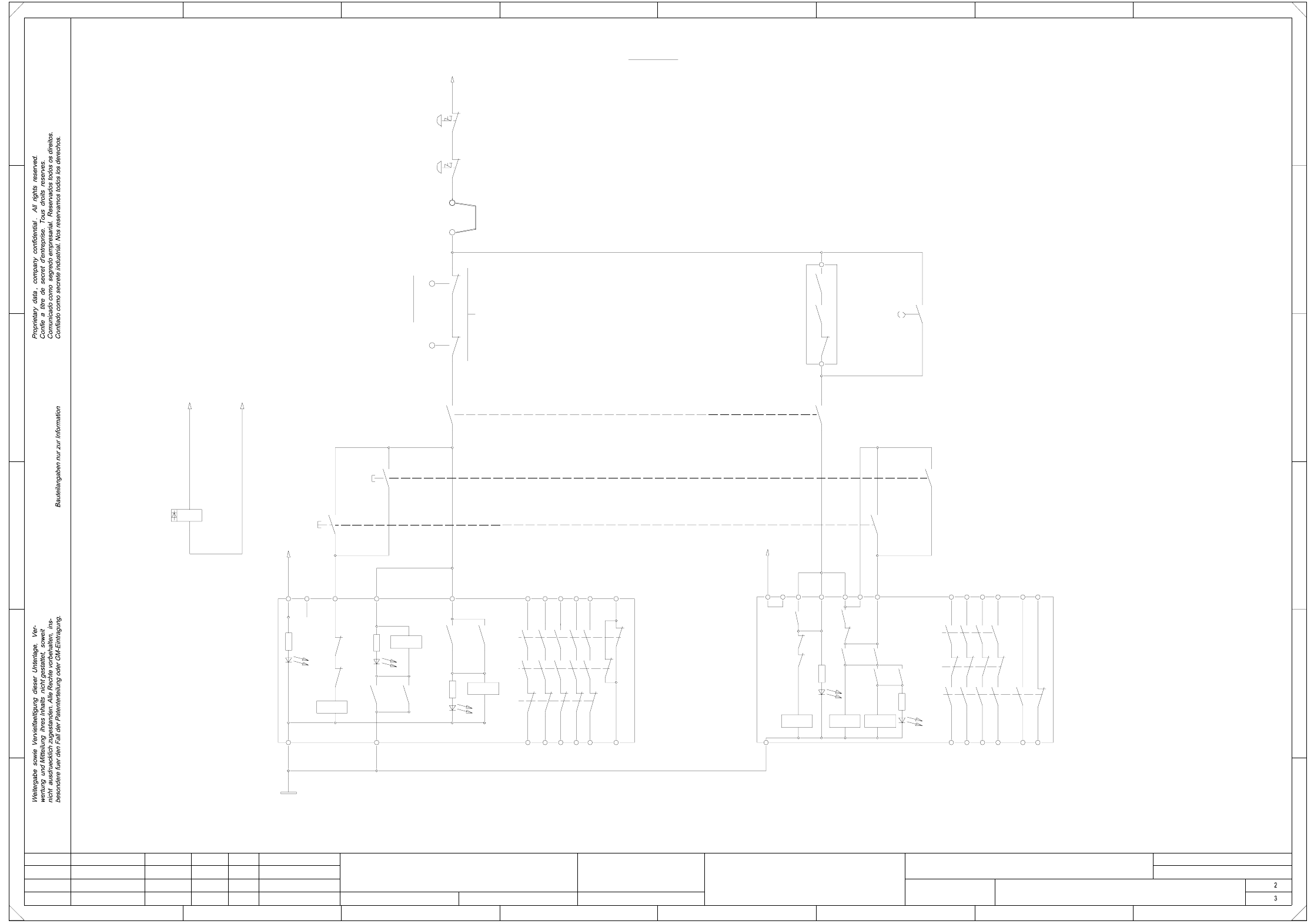
2 Circuit Diagrams 57
00336812-020101FD3 Safety concept, overview (signaling circuit) (Sh. 3 of 3)
3
3
SMD-Placement System Siplace S23
Product status
Doc. status
Function status
(Signaling circuit)
=
Datum
Gepr.
Norm
Bearb.
Blatt
Urspr. Ers. f. Ers. d.NameDatumAenderungZustand
SIEMENS AG
Bl.
+
5
4
Y0907-S3Y0906-S3
Y0907-S2
C0952-K1
K2
K1
Y0906-S2
Y0438-S1
X210
Y0907-S1
Y0906-S1
C0952-K2
C0952-K3
Y0907-S4
Y0413-S1
+24VDC
Monitoring
software release signal
Cover switch
Monitoring
Emergency stop mushroom-head push-button
Monitoring
Monitoring
(Siplace 80F)
Cover switch
(1-n)
Cover switch
External
Output
Input
Control ON
Control ON
123
234567
E
D
C
B
A
OFF button
Monitoring
Monitoring
ON button
Monitoring
key-operated switch
67
Laser
Monitoring
Signaling circuit
Software release signal
Key-operated switch
Input/Output
Output
Input
Leh
Leh
02
01
01
03.09.98
23.01.98
23.01.98
03.09.98
Werner
#
Safety concept overview
00336812-020101FD3
8
1 8
A
B
C
D
E
FF
PL EA1 E
Leh
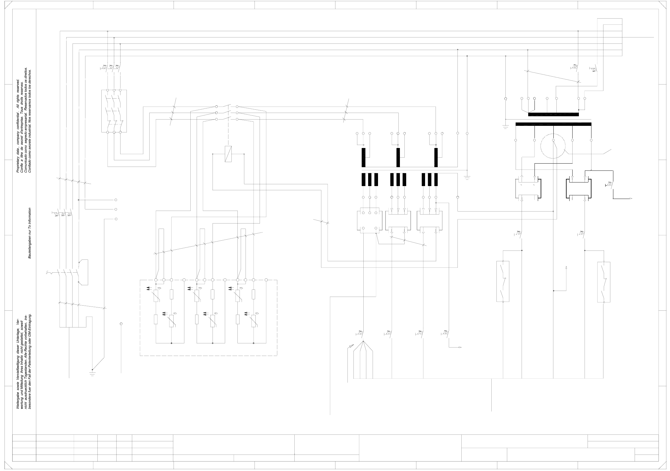
2 Circuit Diagrams 58
00336812-020102LD3 Power supply circuit diagram (Sh. 1 of 2)
10A
4
~~
-
V3
105
105
105
11
12
1L+
1L+
F4
20A
+
~
2
3
5
00324356-xx
K2
7
8
9
10
00300161-06
F8
1
14
2L-
6
7L+
K2
GND
13
F9
10A
2
1
2
10A
B
4L+
5L+
1
2
24V AC
24
40A
+
10A-
34
~~
~~~
13
62
8
PE
16A
PE
F2
3313 23
6
12
48
1L-
13 14 16
48
15
42
42
42
17 18
400
23
0V
19
10A
2
400
208
83
9
V4
+36A
N
PE
7
24
Q1
16A
10A
L3L1 L2 N
T3T1 T2 N’
2414
F10
T2
K1
400
4
5
8
0
11
24
+5%
120
150
4 5
230
230
6
24
48
13
N
X200
3
8
208
400
208
400
7152
400
-5%
PE
F1
1 2
--
~
V5
+
36A
~
6A
2
1
T1
10 9
6
6A
5
F11
1
1
F3
10A
bk
2
N
2
1
2
SMD-Placement System Siplace S23
Product status
Doc. status
Function status
(move wire 3 from terminal 13 to terminal 14
connected in parallel, if the machine is
continue systematically for the other phases)
The inrush current limiter has to be
move wire 2 from terminal 12 to 13
operated at 120V
Jumper is part of the main switch.
Remove jumper if nessecary (IT power
supply) (France, Italy, Japan, U.S.A.)
bk
2,5mm²
2,5
bk
bk
2,5mm²
bk
bk
bk
bk
bk
(Lifting table)
(dp1/Z axes)
bk
per sleeve
gr
rd
bl
bk
4
bk
bk
bk
bl
gnye
gnye
bl
cover for
supply
power
base
To
Power
main power
To
filter 1
gnye
Two wires
2
(Star/lifting table)
(Tape cutter)
C0508-W1 gr
external emergency stop
To sheet 2
2,5mm²
bk
1,5mm²
bk
1,0mm²
To
sheet 2
bk
bk
(Star, slow)
2,5mm²
bk
(X,Y slow)
bk
To sheet 2
1,0mm²
bk
wh
gnye
br
bk
V3(-)
2L-(0V)
2
6
1
3
5
Inrush current limiter
11 12 13
wh
bk
supply
gnye
bl
gnye
4
3
bk
1
switch
Main
2,5mm²
2.5mm²
double-ended ferrule
bk
bk
1,5mm²
mm²
2,5mm²
bk
3
4
5
7
8
9
22
bk
14 21
br
23 24 31 32 33 34
2,5mm²
bk
bk
bk
Join strands
in a
bk
4,0mm²
bk
bk
bk
bk
10,0mm²
terminal panel,
righthand side
2,5mm²
bk
2,5mm²
A1
00342917-XX (W3)
00342917-XX (W1)
gnye
2,5mm²
1,5mm²
Attention !
6
1
2
~
righthand side
terminal panel,
To
To
bk
terminal panel,
To
(X,Y axes)
bk
bk
bk
bk
bk
bk
bk
righthand side
F
E
D
C
B
A
8
A
00341193-xx
00324358-xx
V1
Power supply circuit diagram
24V AC
1
1L+
10
25R
56R
25R
56R
56R
25R
56R
25R
56R
25R
A2(-)
56R
25R
PL EA1 E
K4
A1(+)
=
Datum
Gepr.
Norm
Bearb.
Blatt
Urspr. Ers. f. Ers. d.NameDatumAenderungZustand
SIEMENS AG
Bl.
+
00336812-020102LD3
Leh
Leh
Deu
02
01
02
02.09.98
23.01.98
04.12.98
04.12.98
Werner
#
C
D
E
F
1L+
2L+
3L+
bk
6L+
1
F5
2
10A
2
F6
1
F7
11
4
PE
6
78
1234567
1
3456
V2
-+