RX-8_SPE_EN.pdf - 第23页
19 4-7-5 Board position correcting f unction Board positioning Reference for positioni ng a board Standard specificatio ns (without a stopper): the machin e stops a board at a target position by detecting the board edg e…
18
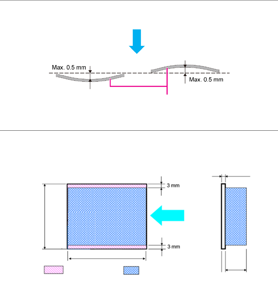
4-7-3 Allowable warpage of a board
4-7-4 Available area for placing a component on the topside and rear side of a board
As shown in the figure below, the machine cannot place any component in the area 3 mm from each
edge of a printed wiring board.
The maximum height of a component mounted on the rear side is 26 mm.
Component placement direction
Board
Flow
direction
Conveyor rail
section
Component installation
range that permits use of
the device
Board D
Board T
Board W
Bottom
side
26 mm
19
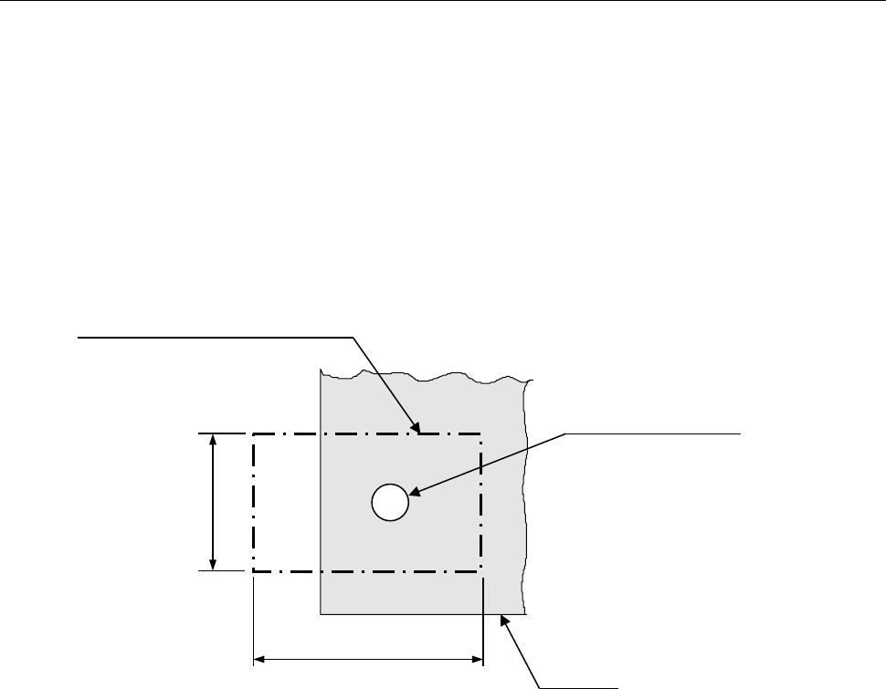
4-7-5 Board position correcting function
Board positioning
Reference for positioning a board
Standard specifications (without a stopper): the machine stops a board at a target position by
detecting the board edge.
Field of vision for recognizing a board reference mark
Field of vision of a camera: 14.2 × 10.7 mm
Depth of focus: ± 2 mm
Note: The values indicating the field of vision are the designed values. They do not match the
values of the actual machine completely.
Size of the window for recognizing a board reference mark
Although this size can be changed, you have to secure a clearance between a recognition mark and
its surrounding area as described in the sections “Shapes and dimensions of a recognition mark”
and “Clearance of a recognition mark.”
How to correct a recognition mark
Reference mark: Two or three (see Note) marks located on a board to correct the entire board.
When the machine detects two reference marks, it corrects the positioning, angle and
expansion/contraction of the entire board. When detecting three reference marks, it corrects the
perpendicularity in the X and Y direction also.
Note: The position of each mark is arbitrary. However, when three marks are located on a board,
they shall not be located in alignment with one another (it is recommended to locate these marks at
any of four corners of a board respectively.)
Basic material of a recognition mark
• The material of a recognition mark shall be uncoated copper or coated copper. (See the
description “Coating of a recognition mark” for coating.)
• Strong contrast between the surface of a recognition mark and the material used in adjacent
printed circuits is required.
• Any recognition mark shall not be oxidized and its material shall not become inferior.
Coating of a recognition mark
The surface of a recognition mark shall be coated as follows:
• Copper foil (may not be recognized depending on its oxidation or corrosion state.)
• Solder coat (may not be recognized depending on the solder shape or its surface condition.)
14.2 mm
10. 7 mm
Recognition mark
Board
Field of view for recognizing a board
20
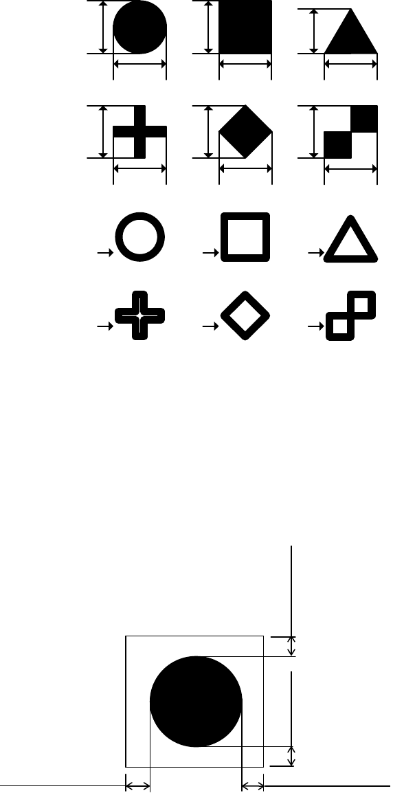
Shapes and dimensions of a recognition mark
A recognition mark shall conform to JIS C5010 “General rules for printed wiring boards” and
JPCA-PB01-2004 “Printed Wiring Boards.”
The standard marks represent 12 shapes as shown in the following figure, “Shapes of recognition
marks.”
Shapes of recognition marks
A
A
A
A
A
A
A
A
A
A
A
A
B
B
B
B
B
B
A: 0.4 mm or more but 2.0 mm or less
B: Width of 0.2 mm or more
The size of mark is limited.
Clearance of a recognition mark
There shall be a space in which any other marks such as a conductor pattern, a solder resist and a
marking are not located around each recognition mark. It is preferable that the dimensions of this
space are larger than those of a square by 0.5 mm or more viewed from the outside of a recognition
mark.
Clearance of a recognition mark
0.5 mm or more
0.5 mm or more
0.5mm or more 0.5 mm or more