KE-3010A_SPE_EN.pdf - 第23页
- 18 - 4.6. Component Plac ement Accurac y *1 T he regulated value of a component to be recogniz ed with laser is “Cpk ≥ 1.” *2 The placement accuracy that can be obtained when a placement position is cor r ected by reco…
- 17 -
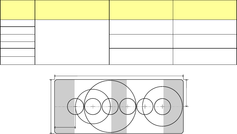
Note 13: The size of a component to be recognized with each nozzle is shown in the table below.
Nozzle
number
Simultaneous measurement
Clearance
(Between the laser surface
and a component)
Applicable component
size
1
0.40 x 0.20 mm to □10.00 mm
(Diameter: 15.0 mm or less)
2.15 mm □20.00mm (See Note 14.)
2
3
2.81 mm □33.50 mm
4
5
2.15 mm □20.00 mm (See Note 14.)
6
#1
#2
#3
#4
#5
#6
26.5
53.0
120.0
17.5
Note 14: □22.5 mm to□ 33.5mm can be used in L3 or L4 only.
Note 15: Even thoguh the size exceeds
□ 20 mm,
a component whose size is 24 mm×11 mm is applicable.
Note 16: The minimum component height does not affect recognition of a component with a VCS.
It shall be recognized with the CDS.(KE-3020V only)
Note 17: When the component size is less than
□ 3 mm,
recognize and place the component on a board with an LNC60 head.
Note 18: To recognize the image of a resistor chip, trimmer, SOT or LED component whose size is
from 1.0×0.5 mm to
□ 3mm with a VCS, recognize it as a general-purpose vision
component.
- 18 -
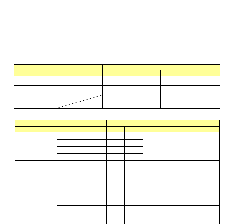
4.6. Component Placement Accuracy
*1 The regulated value of a component to be recognized with laser is “Cpk ≥ 1.”
*2 The placement accuracy that can be obtained when a placement position is corrected
by recognizing component image shall be the absolute value from the component
reference mark or PWB reference mark.
*3 The placement accuracy of a 0402 component described below is realized if local
fiducial marks are used, the distance between two marks is 20 mm or less, and a 0402
component is placed within the mark.
(1) Placed positions (X, Y)
(Unit:μm)
Laser
Vision (VCS)
LNC60 FMLA MNVC IC head
Square chip
0402, 0603
± 50 ― ― ―
Square chip
1005 or bigger
± 50 ± 50 ― ―
QFP
(Pitch: 0.5, 0.4, 0.3)
± 40
(When a component positioning
mark is used)
± 30
(When a component positioning mark
is used)
(2) Placed posture (
θ
) (Unit:°)
Laser Vision (VCS)
LNC60
FMLA
MNVC
IC head
Square chip
0402 ±5.0 ―
― ―
0603 ±3.0 ―
1005 ±2.5 ±2.5
1608 or more ±2.0 ±2.0
QFP
(Pitch: 0.5, 0.4, 0.3)
50 mm or more ― ― - ±0.04
From 40 mm to less than 50 mm
― ― - ±0.05
From 30 mm to less than 40 mm
― ― ± 1.11 ±0.07
From 20 mm to less than 30 mm
― ― ±0.12 ±0.1
From 10 mm to less than 20 mm
― ― ±0.22 ±0.2
10 mm or less
―
―
±0.33
±0.3
Adjacent pitch
- 0402: 0.15 mm
- 0603: 0.20 mm
- 19 -
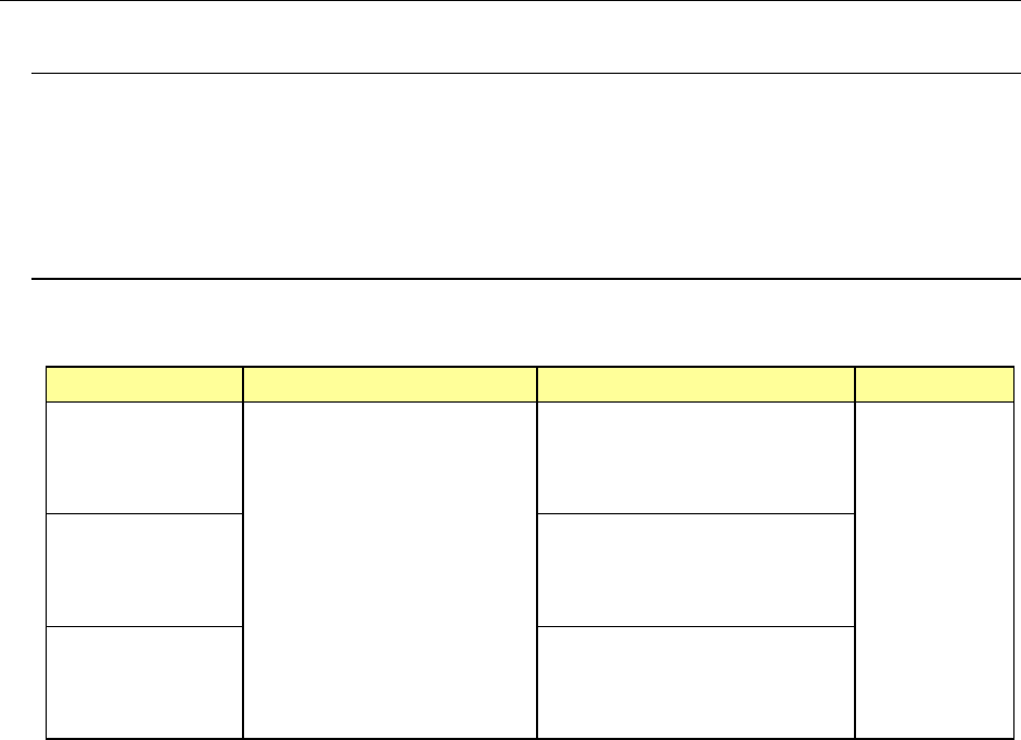
4.7. Applicable PWBs
4.7.1. PWBs transport direction
Rightward flow (transporting from left to right, looking from the front side)
Leftward flow (transporting from right to left, looking from the front side)
Note
:
This direction is set at the factory (Factory-set).
4.7.2. PWB sizes and Mass
(1) PWB sizes
(Unit: mm)
Minimum size (D
1
x W
1
) Maximum size (D
2
x W
2
) Thickness T
M PWB
specification
50×30
(When the auto PWB width
adjusting function is provided:
50 x 50)
330×250
(When a function applicable to
long PWB is provided: 650 x
250)
0.3~4.0
L-PWB
specification
410×360
(When a function applicable to
long PWB is provided:
800 x 360)
L-Wide
specification
510×360
(When a function applicable to
long PWB is provided:
1010 x 360)
Note 1: “D” indicates the dimension in the board transport direction, and “W” indicates the
direction perpendicular with “D” W/D should be 2 or less.
Note 2: Contact us for a notched board or board whose shape is irregular.
Note 3: A PWB whose reflection ratio is low may not be able to be detected regardless of its
material or color.
(2) Maximum allowance of PWB mass :2,000 g
(3) Allowable warpage of a PWB
0.2 mm or less per 50 mm area, and 1 mm or less for both upper and lower directions
(these values conform to the JIS B 8461 regulation.)