JX-100_SPE_EN06.pdf - 第18页
4.7.5.2 Dimensions and tolerances The outside dimensions shall range from 0.5 mm up to 3.0mm, whose tolerance, less than 10%. For all the inside-blank forms, the edging line wid th shall be more than 0.2 mm. 0.2 mm or mo…
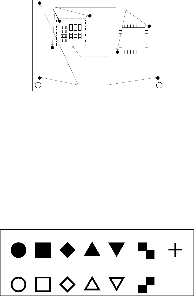
搭
載グループ
基準マーク
部品位置決めマーク
エリア部品位置決めマーク
Component placement
rea positioning marks a
Placement group
PWB reference marks
Component
positioning marks
Figure 7 Reference marks and components positioning marks
4.7.5 Shapes of each mark to be recognized
Marks to be recognized conform to the EIAJ ET-7302 “Recognition Marks for Surface
Mounting PWB.”
4.7.5.1 Forms
- The standard marks represent the thirteen (13) forms as shown in the following block,
“forms of recognition marks.”
- For any mark other than those shown in the said block, customers shall make
templates to allow for recognition through a pattern matching.
Note 1: Limited to the standard marks only
;
and any area fiducial mark is excluded
from the subjects.
Note 2: Within a field of vision, there should be no similar form pattern other than
the subjected form patterns.
- For regular triangles, checker patterns and users’ templates, the 90°up-side-down
marks can also be recognized.
Circle Square Diamond
Regular
triangle
Up-side-down
triangle
Checker
pattern
Cross
Inside-blank
circle
Inside-blank
square
Inside-blank
diamond
Inside-blank
up-side-down
triangle
Checker
pattern
Inside-blank
Regular
triangle
Figure 8 Forms of Recognition Marks
13
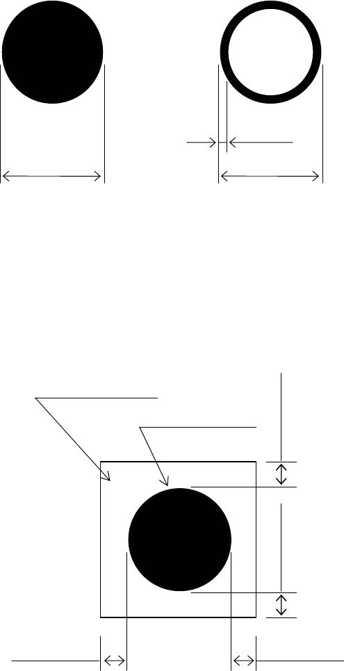
4.7.5.2 Dimensions and tolerances
The outside dimensions shall range from 0.5 mm up to 3.0mm, whose tolerance, less
than 10%.
For all the inside-blank forms, the edging line width shall be more than 0.2 mm.
0.2 mm or more
0.5 to 3.0mm
0.5 to 3.0mm
Figure 9 Dimensions and tolerances of recognition marks.
4.7.5.3 Clearance
It is desirable that there is, around each recognition mark, a space having nothing of
such other marks as conductor pattern, solder resist, marking and the like, and that this
space dimensions is a larger square than the mark by 0.5 mm or more from the outer
circumference of the recognition marks.
0.5 mm or more
0.5 mm or more 0.5 mm or more
0.5 mm or more
Recognition mark
Clearance area
Figure 10 Clearances of recognition marks
14
4.7.5.4 Basic quality of recognition marks
- Copper not coated or coated
- It needs to have a clear contrast between the recognition mark surface and the print
wiring quality.
- It needs to have neither oxidation nor quality deterioration of the recognition marks.
4.7.5.5 Coating the recognition marks
The recognition mark surfaces shall all be coated as follows:
- Transparent antioxidant coating
- Nickel plating
- Tin plating
- Solder plating
- Gold plating
- Hot air repeller solder coating
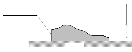
4.7.5.6 Flatness
The difference in height of the surface of a recognition mark shall be 0.015 mm or less.
For flux, there shall be no unevenness of applied flux.
0.015mm
以内
認識マーク
or less
Recognition mark
基板
Board
Figure 11 Cross section and difference in height of a recognition mark
15