JX-100_SPE_EN06.pdf - 第19页
4.7.5.4 Basic quality of recognition marks - Copper not coated or coated - It needs to have a clear contrast between the recognition mark surface and the print wiring quality . - It needs to have neither oxidation nor qu…
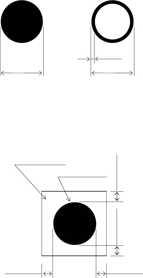
4.7.5.2 Dimensions and tolerances
The outside dimensions shall range from 0.5 mm up to 3.0mm, whose tolerance, less
than 10%.
For all the inside-blank forms, the edging line width shall be more than 0.2 mm.
0.2 mm or more
0.5 to 3.0mm
0.5 to 3.0mm
Figure 9 Dimensions and tolerances of recognition marks.
4.7.5.3 Clearance
It is desirable that there is, around each recognition mark, a space having nothing of
such other marks as conductor pattern, solder resist, marking and the like, and that this
space dimensions is a larger square than the mark by 0.5 mm or more from the outer
circumference of the recognition marks.
0.5 mm or more
0.5 mm or more 0.5 mm or more
0.5 mm or more
Recognition mark
Clearance area
Figure 10 Clearances of recognition marks
14
4.7.5.4 Basic quality of recognition marks
- Copper not coated or coated
- It needs to have a clear contrast between the recognition mark surface and the print
wiring quality.
- It needs to have neither oxidation nor quality deterioration of the recognition marks.
4.7.5.5 Coating the recognition marks
The recognition mark surfaces shall all be coated as follows:
- Transparent antioxidant coating
- Nickel plating
- Tin plating
- Solder plating
- Gold plating
- Hot air repeller solder coating
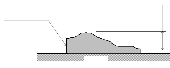
4.7.5.6 Flatness
The difference in height of the surface of a recognition mark shall be 0.015 mm or less.
For flux, there shall be no unevenness of applied flux.
0.015mm
以内
認識マーク
or less
Recognition mark
基板
Board
Figure 11 Cross section and difference in height of a recognition mark
15
5. STANDARD FUNCTIONS AND OPTIONS
5.1 Standard functions
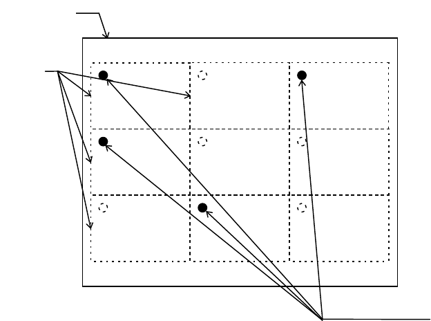
5.1.1 Bad mark recognition
Recognition can be performed by OCC.
A bad mark is given to a circuit on a multi-circuit PWB to prevent any component from
being placed on the circuit.
The size of the mark should be φ2.5 mm or more and clear contrast with the PWB color
is required.
If there is a difference in reflected light quantity between the PWB color and the mark
color, the brightness/darkness for the PWB color must be switched.
基板
回路
Board
Circuits
バッドマーク
Bad marks
Figure 12 Bad mark types
5.1.2 Liquid crystal touch panel
This is an input device to operate the device by touching the screen. This device can be
operated intuitively to improve the operability.
5.2 Options
5.2.1 Feeder floating detecting sensor (Option for the factory setting)
This sensor is used to avoid mechanical trouble that may be caused when the tape feeder,
stick feeder, or bulk feeder cannot be mounted correctly.
When the sensor detects a floating status, the XY axis movement is stopped and a warning is
given to the operator
. (JX-100: Option for both front and rear, JX-100 LED: Standard for
front but Option for rear.)
16