Printer 600 Machine Controller.pdf - 第34页
0$&+,1( &21752//( 5 '8$/67( 33(5'5,9( 6.34 Technical Reference Manual Chapter Issue 4 May 03 Output Signals Each micro co ntroller is preprog rammed with a machi ne code tha t utilizes the directi on…

0$&+,1(&21752//(5
'8$/67(33(5'5,9(
Chapter Issue 4 May 03 Technical Reference Manual 6.33
DUAL STEPPER DRIVE
The dual stepper drive card can be configured to drive either a single or two
stepper motors. For single axis control, the drive cards are not populated with
two device sets.
Stepper drive signal coding is generated by two on board OTP-EPROM 8-Bit
CMOS Micro-controllers (PIC16C54). The drive to each stepper motor phase
is provided by two H-Bridge motor driver devices (LMD 18245).
Circuit Protection The circuit is connected to the + 24V SW (Switched) and the + 24V US
(UnSwitched) supplies. The unswitched supply is protected by a diode-fuse
voltage transient suppressor circuit consisting of D2 and F1(0.5AT). The diode
operates over an extremely short time period, this enables the absorption of
voltage spikes without blowing the fuse. If a sustained current is experienced
the fuse exceeds its rated value and blows. The switched supply is similarly
protected by a diode-fuse circuit consisting of D1 and F2 (3.15AT)
Regulated Supply The +5V regulated voltage (VCC) is provided by the +24V US voltage at the
output of U7. This voltage in turn provides the CH1 and CH2 reference voltages
for the LMD 18245 DAC Ref, this output is used as a comparator voltage in the
device’s internal 4-Bit digital to analog converter.
Input Signals Two inputs, Dir 1 and Dir 2 are the direction inputs and Step 1 and Step 2 are
the step signals to the stepper drive motors. These signals are opto coupled
through the input device U3 (TLP 521 - 4) then routed to the respective micro
controller devices (PIC16C54) and test points TP1-4.
0$&+,1(&21752//(5
'8$/67(33(5'5,9(
6.34 Technical Reference Manual Chapter Issue 4 May 03
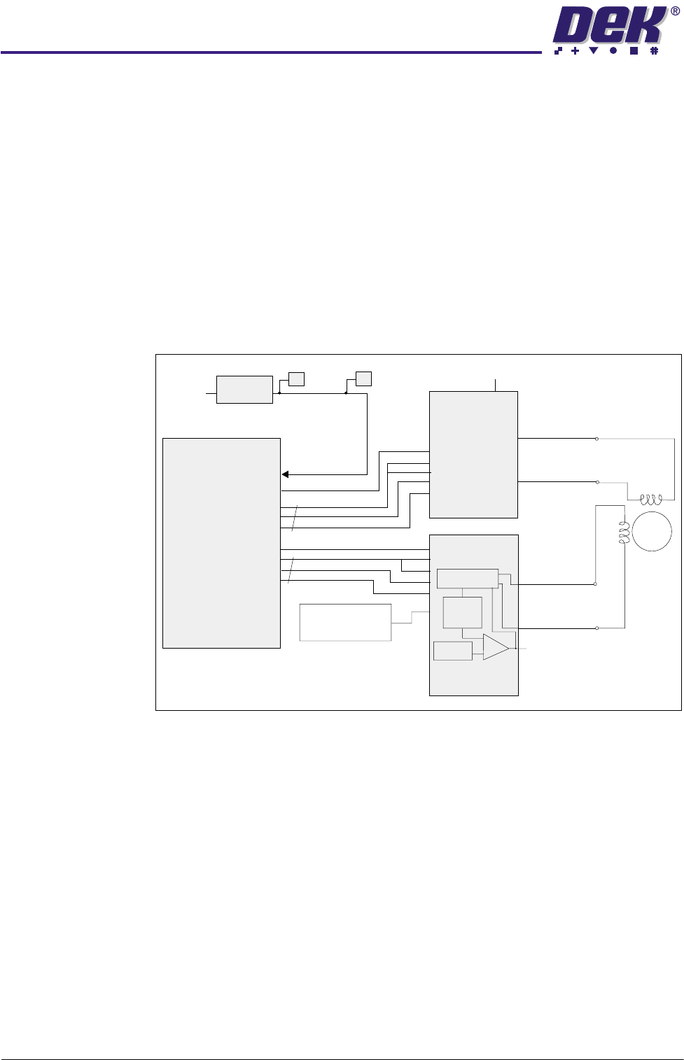
Output Signals Each micro controller is preprogrammed with a machine code that utilizes the
direction and step data from the multiplexer (MUX Dir/Step), to sequence the
stepper drive signals (RB0-7). These signals are fed to two LMD 18245 devices.
The LMD devices each form a bi-polar chopper amplifier stage providing single
phase drive to one half of the stepper motor (CHxA+ and CHxA-) or (CHxB+
and CHxB-) windings. Outputs RB0 and RB4 provide the direction data and are
utilized in the chopper circuit to switch the H-Bridge power switches and hence
the current direction in the phase winding. The LMD device compares the DAC
reference voltage mentioned previously with the output of the current sense
amplifier this is connected to the jumper links - JP3, 4, 5, 6, 9, 10, 11 and 12.
The links are all factory set to achieve either half step 1A/phase or half step 2A/
phase outputs. The actuators and the paste dispense stepper motors are rated
at 1A/phase. The squeegee motors, the moving rail motors are rated at 2A/
phase.
Figure 6-24 Dual Stepper Block Diagram
Microcontroller
RA0-RA1
Dir
Dir
RB0
RB1/2/3
RB4
RB5/6/7
{
{
CHxA+
24VSW
Rotor
CHxB+
CHxA-
CHxB-
TP1
or TP3
TP2
or TP4
+5V Reference
Voltage
H-Bridge
Chopper
Amplifier
H-Bridge
Stepper
Motor
NOTE
Both halves are identical.
LMD 18245
LMD 18245
PIC16C54
DAC
I
Sense
I/P Buffer
Step/Dir
0$&+,1(&21752//(5
'8$/67(33(5'5,9(
Chapter Issue 4 May 03 Technical Reference Manual 6.35
Stepper Drive Card
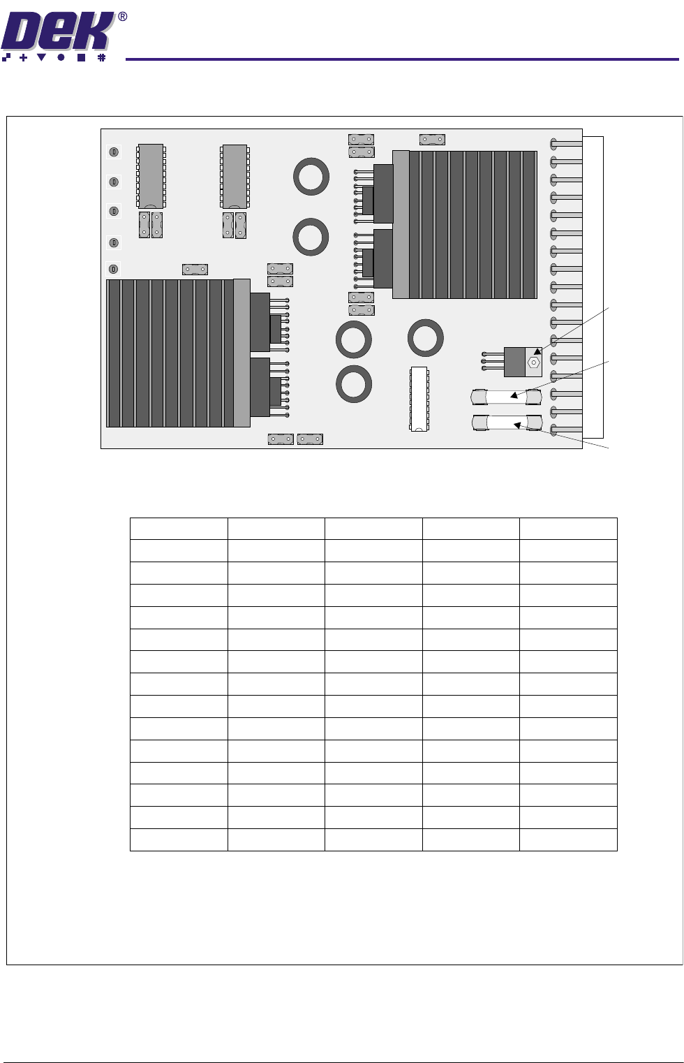
Figure 6-25 Dual Stepper Drive PCB
Fuse F1 -
0.5AT
Fuse F2-
3.15AT
+5V
Regulator
TP4 - Step 2
TP5-0V
TP2 - Step 1
TP3 - Dir 2
TP1 - Dir 1
JP11
JP3
JP4
JP9
JP10
JP5
JP1
JP2
JP7
JP8
JP6
JP14
JP12
JP13
Jumper Links
Slot X3
Slot X4
Slot X5
Slot X6
X
X
X
X
X
X
X
X
X
X
X
X
JP1
JP2
JP3
JP4
JP5
JP6
JP7
JP8
JP9
JP10
JP11
JP12
JP13
JP14
Dual Stepper Card Configuration Table
NOTE
denotes jumper link fitted.
X
CAUTION
ANTI STATIC HANDLING. Standard precautions must be adhered to when handling
electronic cards and configuring and inserting cards into enclosures.