IPC-SM-782A-表面贴装焊盘图形设计标准.pdf.pdf - 第119页
5.0 LAND PATTERN DIMENSIONS Figure 3 provides the land pattern dimensions for SOIC com- ponents. These numbers represent industry consensus on the best dimensions based on empirical knowledge of fabricated land patterns.…
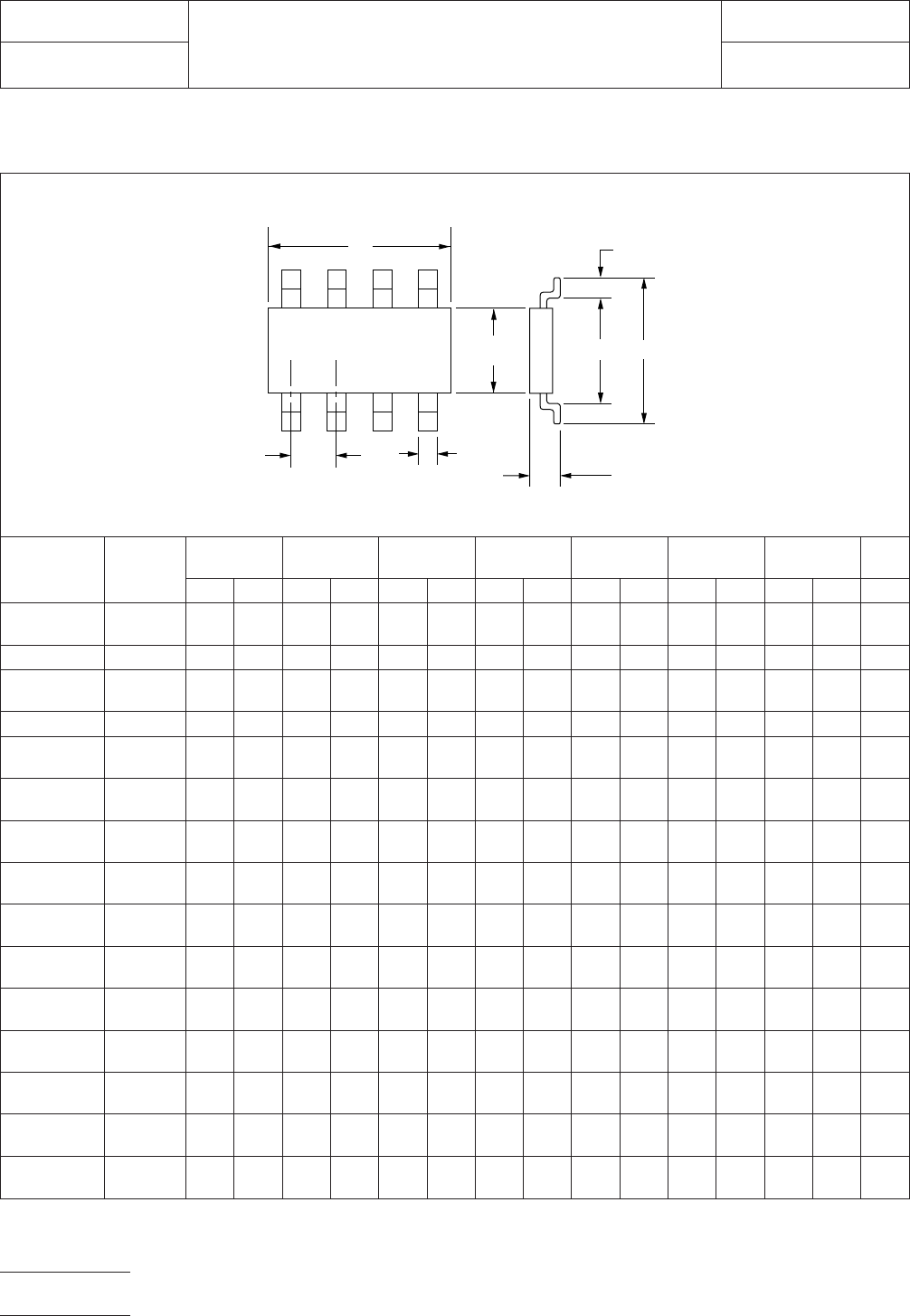
4.0 COMPONENT DIMENSIONS
Figure 2 provides the component dimensions for SOIC components.
Component
Identifier
JEDEC
Number
L (mm) S (mm) W (mm) T (mm) A (mm) B (mm) H (mm)
P
(mm)
min max min max min max min max min max min max min max basic
S08 MS-012
AA
5.80 6.20 3.26 4.55 0.33 0.51 0.40 1.27 3.80 4.00 4.80 5.00 1.35 1.75 1.27
S08W — 10.00 10.65 7.46 8.85 0.33 0.51 0.40 1.27 7.40 7.60 5.05 5.45 2.35 2.65 1.27
S014 MS-012
AB
5.80 6.20 3.26 4.55 0.33 0.51 0.40 1.27 3.80 4.00 8.55 8.75 1.35 1.75 1.27
S014 W — 10.00 10.65 7.46 8.85 0.33 0.51 0.40 1.27 7.40 7.60 8.80 9.20 2.35 2.65
S016 MS-012
AC
5.80 6.20 3.26 4.55 0.33 0.51 0.40 1.27 3.80 4.00 9.80 10.00 1.35 1.75 1.27
S016W MS-013
AA
10.00 10.65 7.46 8.85 0.33 0.51 0.40 1.27 7.40 7.60 10.10 10.50 2.35 2.65 1.27
S020W MS-013
AC
10.00 10.65 7.46 8.85 0.33 0.51 0.40 1.27 7.40 7.60 12.60 13.00 2.35 2.65 1.27
S024W MO-119
AA
10.29 10.64 8.21 9.01 0.36 0.51 0.53 1.04 7.40 7.60 15.54 15.85 2.34 2.64 1.27
S024X MO-120
AA
11.81 12.17 9.73 10.54 0.36 0.51 0.53 1.04 8.76 9.02 15.54 15.85 2.34 2.64 1.27
S028W MO-119
AB
10.29 10.64 8.21 9.01 0.36 0.51 0.53 1.04 7.40 7.60 18.08 18.39 2.34 2.64 1.27
S028X MO-120
AB
11.81 12.17 9.73 10.54 0.36 0.51 0.53 1.04 8.76 9.02 18.08 18.39 2.34 2.64 1.27
S032W MO-119
AC
10.29 10.64 8.21 9.01 0.36 0.51 0.53 1.04 7.40 7.60 20.62 20.93 2.34 2.64 1.27
S032X MO-120
AC
11.81 12.17 9.73 10.54 0.36 0.51 0.53 1.04 8.76 9.02 20.62 20.93 2.34 2.64 1.27
S036W MO-119
AD
10.29 10.64 8.21 9.01 0.36 0.51 0.53 1.04 7.40 7.60 23.16 23.47 2.34 2.64 1.27
S036X MO-120
AD
11.81 12.17 9.73 10.54 0.36 0.51 0.53 1.04 8.76 9.02 23.16 23.47 2.34 2.64 1.27
Figure 2 SOIC component dimensions
P
H
SL
W
B
A
T
IPC-782-9-1-2
IPC-SM-782A
Subject
SOIC
Date
5/96
Section
9.1
Revision
A
Page2of4
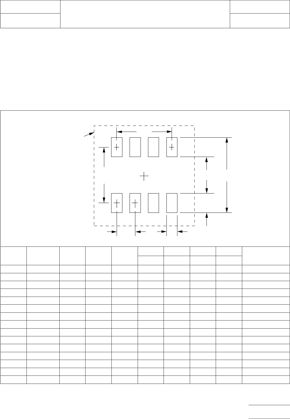
5.0 LAND PATTERN DIMENSIONS
Figure 3 provides the land pattern dimensions for SOIC com-
ponents. These numbers represent industry consensus on the
best dimensions based on empirical knowledge of fabricated
land patterns.
In the table, the dimensions shown are at maximum material
condition (MMC). The least material condition (LMC) should
not exceed the fabrication (F) allowance shown on page 4.
The LMC and the MMC provide the limits for each dimension.
The dotted line in Figure 3 shows the grid placement court-
yard which is the area required to place land patterns and
their respective components in adjacent proximity without
interference or shorting. Numbers in the table represent the
number of grid elements (each element is 0.5 by 0.5 mm) in
accordance with the international grid detailed in IEC publica-
tion 97.
RLP No.
Component
Identifier Z (mm) G (mm) X (mm)
Y (mm) C (mm) D (mm) E (mm)
Placement Grid
(No. Grid
Elements)
ref ref ref ref
300A S08 7.40 3.00 0.60 2.20 5.20 3.81 1.27 16x12
301A S08W 11.40 7.00 0.60 2.20 9.20 3.81 1.27 24x12
302A S014 7.40 3.00 0.60 2.20 5.20 7.62 1.27 16x20
303A S014W 11.40 7.00 0.60 2.20 9.20 7.62 1.27 24x20
304A S016 7.40 3.00 0.60 2.20 5.20 8.89 1.27 16x22
305A S016W 11.40 7.00 0.60 2.20 9.20 8.89 1.27 24x22
306A S020W 11.40 7.00 0.60 2.20 9.20 11.43 1.27 24x28
307A S024W 11.40 7.00 0.60 2.20 9.20 13.97 1.27 24x32
308A S024X 13.00 8.60 0.60 2.20 10.80 13.97 1.27 28x32
309A S028W 11.40 7.00 0.60 2.20 9.20 16.51 1.27 24x38
310A S028X 13.00 8.60 0.60 2.20 10.80 16.51 1.27 28x38
311A S032W 11.40 7.00 0.60 2.20 9.20 19.05 1.27 24x44
312A S032X 13.00 8.60 0.60 2.20 10.80 19.05 1.27 28x44
313A S036W 11.40 7.00 0.60 2.20 9.20 21.59 1.27 24x48
314A S036X 13.00 8.60 0.60 2.20 10.80 21.59 1.27 28x48
Figure 3 SOIC land pattern dimensions
x
GZ
Y
E
D
C
Grid
placement
courtyard
IPC-782-9-1-3
IPC-SM-782A
Subject
SOIC
Date
5/96
Section
9.1
Revision
A
Page3of4
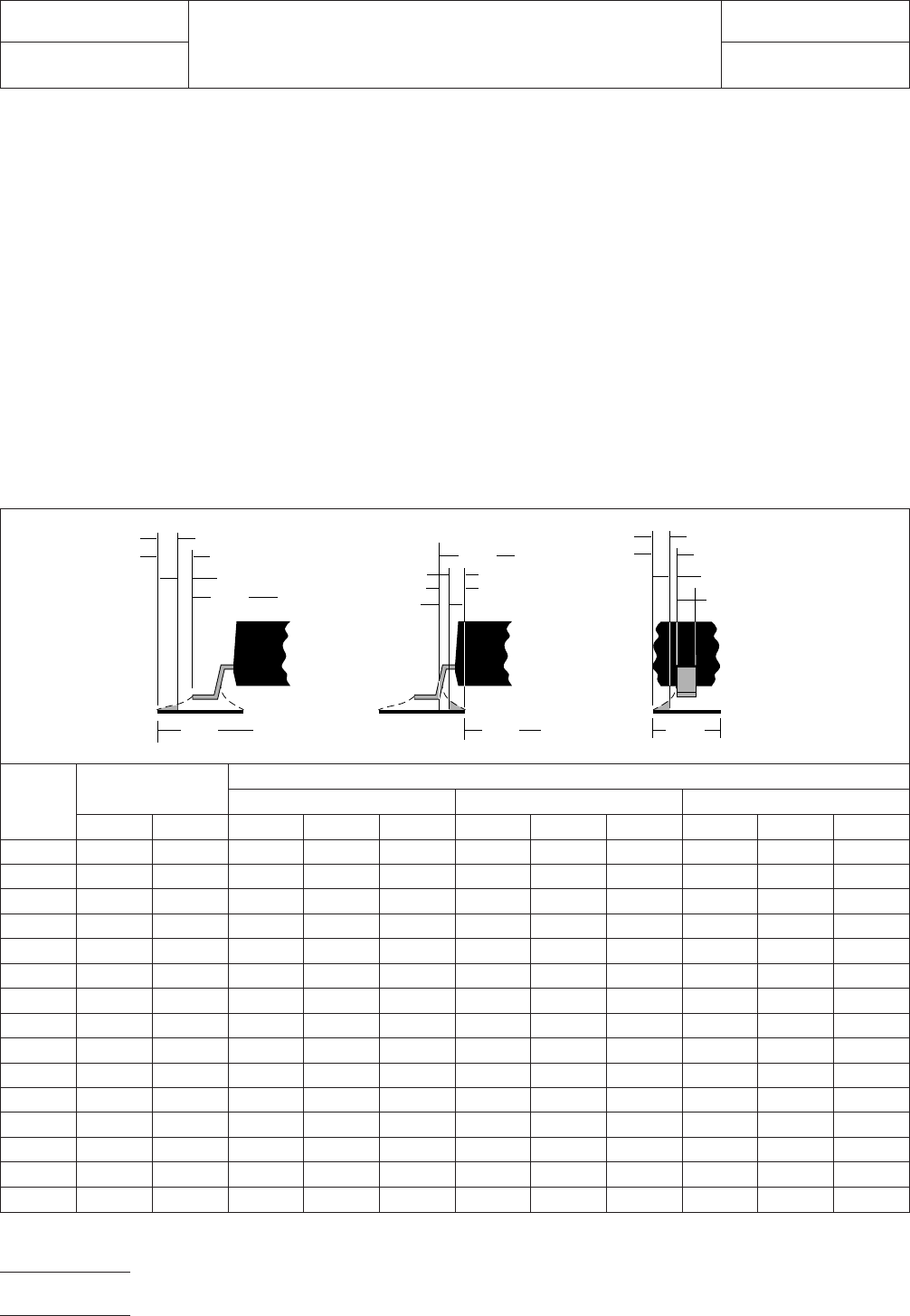
6.0 TOLERANCE AND SOLDER JOINT ANALYSIS
Figure 4 provides an analysis of tolerance assumptions and
resultant solder joints based on the land pattern dimensions
shown in Figure 3. Tolerances for the component dimensions,
the land pattern dimensions (fabrication tolerances on the
interconnecting substrate), and the component placement
equipment accuracy are all taken into consideration.
Figure 4 provides the solder joint minimums for toe, heel, and
side fillets, as discussed in Section 3.3. The tolerances are
addressed in a statistical mode, and assume even distribution
of the tolerances for component, fabrication, and placement
accuracy.
Individual tolerances for fabrication (‘‘F’’) and component
placement equipment accuracy (‘‘P’’) are assumed to be as
given in the table. These numbers may be modified based on
user equipment capability or fabrication criteria. Component
tolerance ranges (C
L
,C
S
, and C
W
) are derived by subtracting
minimum from maximum dimensions given in Figure 2. The
user may also modify these numbers, based on experience
with their suppliers. Modification of tolerances may result in
alternate land patterns (patterns with dimensions other than
the IPC registered land pattern dimensions).
The dimensions for minimum solder fillets at the toe, heel, or
side (J
T
,J
H
,J
S
) have been determined based on industry
empirical knowledge and reliability testing. Solder joint
strength is greatly determined by solder volume. An observ-
able solder fillet is necessary for evidence of proper wetting.
Thus, the values in the table usually provide for a positive sol-
der fillet. Nevertheless, the user may increase or decrease the
minimum value based on process capability.
RLP No.
Tolerance
Assumptions (mm)
Solder Joint
Toe (mm) Heel (mm) Side (mm)
FPC
L
J
T
min J
T
max C
S
J
H
min J
H
max C
W
J
S
min J
S
max
300A 0.10 0.10 0.40 0.59 0.80 1.29 0.13 0.78 0.18 0.02 0.14
301A 0.10 0.10 0.65 0.37 0.70 1.39 0.23 0.93 0.18 0.02 0.14
302A 0.10 0.10 0.40 0.59 0.80 1.29 0.13 0.78 0.18 0.02 0.14
303A 0.10 0.10 0.65 0.37 0.70 1.39 0.23 0.93 0.18 0.02 0.14
304A 0.10 0.10 0.40 0.59 0.80 1.29 0.13 0.78 0.18 0.02 0.14
305A 0.10 0.10 0.65 0.37 0.70 1.39 0.23 0.93 0.18 0.02 0.14
306A 0.10 0.10 0.65 0.37 0.70 1.39 0.23 0.93 0.18 0.02 0.14
307A 0.10 0.10 0.35 0.37 0.56 0.80 0.60 1.01 0.15 0.02 0.12
308A 0.10 0.10 0.36 0.40 0.60 0.81 0.56 0.97 0.15 0.02 0.12
309A 0.10 0.10 0.35 0.37 0.56 0.80 0.60 1.01 0.15 0.02 0.12
310A 0.10 0.10 0.36 0.40 0.60 0.81 0.56 0.97 0.15 0.02 0.12
311A 0.10 0.10 0.35 0.37 0.56 0.80 0.60 1.01 0.15 0.02 0.12
312A 0.10 0.10 0.36 0.40 0.60 0.81 0.56 0.97 0.15 0.02 0.12
313A 0.10 0.10 0.35 0.37 0.56 0.80 0.60 1.01 0.15 0.02 0.12
314A 0.10 0.10 0.36 0.40 0.60 0.81 0.56 0.97 0.15 0.02 0.12
Figure 4 Tolerance and solder joint analysis
Zmax
Lmin
▼
▼
▼
▼
1
/2 T
T
J
T
min
Smax
J
H
min
1
/2 T
H
Xmax
▼
▼
Toe Fillet
▼
▼
▼
Heel Fillet
Side Fillet
▼
▼
▼
▼
▼
J
T
max
J
H
max
J
S
min
▼
▼
▼
▼
▼
▼
▼
▼
▼
▼
▼
▼
▼
▼
▼
Gmin
▼
1
/2 T
S
J
S
max
▼
▼
▼
Wmin
▼
IPC-782-9-1-4
IPC-SM-782A
Subject
SOIC
Date
5/96
Section
9.1
Revision
A
Page4of4