IPC-SM-782A-表面贴装焊盘图形设计标准.pdf.pdf - 第186页
Page Intentionally Left Blank IPC-SM-782 Subject DIPs Date 8/93 Section 13.0 Revision P a g e2o f2

1.0 INTRODUCTION
This section covers land patterns for DIPs (Modified Dual-In-
Line components). Each subsection contains information in
accordance with the following format:
1.0 Scope
2.0 Applicable Documents
3.0 General Component Description (Figure 1)
4.0 Component Dimensions (Figure 2)
5.0 Land Pattern Dimensions (Figure 3)
6.0 Tolerance and Solder Joint Analysis (Figure 4)
The following is the table of contents for this section:
Table of Contents
Modified Dual-In-Line Components
Section Component Standard Source
13.1 DIP JEDEC Publication 95
2.0 APPLICABLE DOCUMENTS
The following documents, of the issue in effect on the revision
date of this section, form a part of this specification to the
extent specified herein.
2.1 Electronic Industries Association (EIA)
1
EIA-481-A Taping of Surface Mount Components for Auto-
matic Placement
EIA-481-2 16 mm and 24 mm Embossed Carrier Taping of
Surface Mount Components for Automated Handling
EIA-481-3 32 mm, 44 mm, and 56 mm Embossed Carrier
Taping of Surface Mount Components for Automated Han-
dling
JEDEC Publication Registered and Standard Outlines for
Solid State and Related Products:
Outline Issue Title
MS-001 C Standard Dual-In-Line Family, 0.300
in. Row Spacing (Plastic)
MS-010 B Standard Dual-In-Line Family, 0.400
in. Row Spacing (Plastic)
MS-011 B Standard Dual-In-Line Family, 0.600
in. Row Spacing (Plastic)
2.2 International Electrotechnical Commission (IEC)
2
IEC 97 Grid Elements
3.0 GENERAL INFORMATION
3.1 General Component Description
A method of modi-
fying DIPs for surface mounting is the ‘‘I’’ mounting technique.
This involves simply cutting the DIP leads to a short length and
placing the device on a pattern of lands to be soldered along
with the other surface mounted devices.
1. Application for copies should be addressed to Global Engi-
neering Documents, 1990 M St. N.W., Washington, DC
20036.
2. Application for copes should be addressed to IEC, 3 rue
de Varembe, PO Box 131 - 1211 Geneva 20, Switzerland
IPC-SM-782
Surface Mount Design
and Land Pattern Standard
Date
8/93
Section
13.0
Revision Subject
DIPs
Page1of2

Page Intentionally Left Blank
IPC-SM-782
Subject
DIPs
Date
8/93
Section
13.0
Revision
Page2of2
1.0 SCOPE
This subsection provides the component and land pattern
dimensions for DIPs (Modified Dual-In-Line components).
Basic construction of the DIP device is also covered. At the
end of this subsection is a listing of the tolerances and target
solder joint dimensions used to arrive at the land pattern
dimensions.
2.0 APPLICABLE DOCUMENTS
See Section 13.0 for documents applicable to the subsec-
tions.
3.0 COMPONENT DESCRIPTIONS
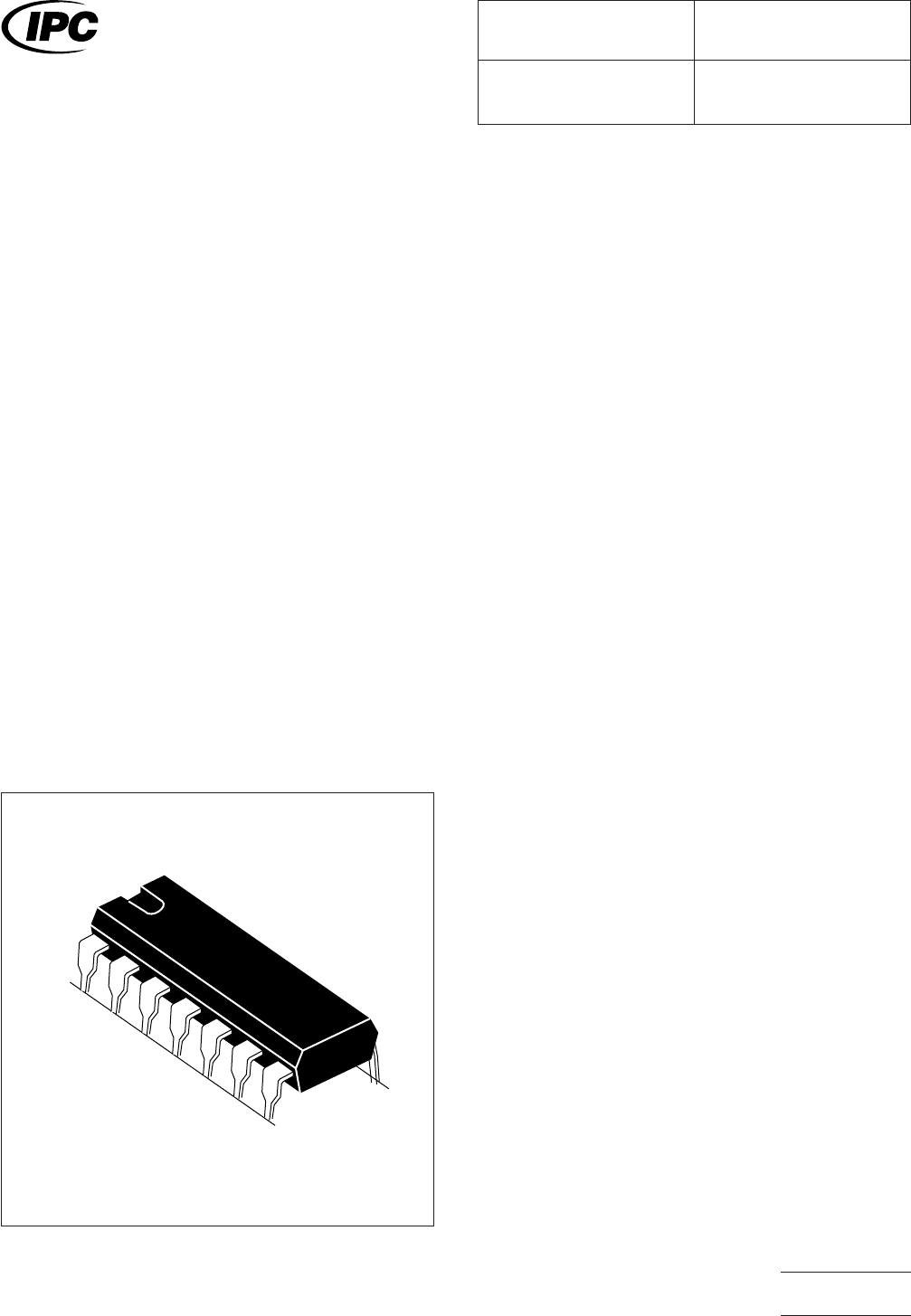
3.1 Basic Construction
See Figure 1. Construction is usu-
ally made of plastic or ceramics.
3.1.1 Termination Materials Leads should be solder-
coated with a tin/lead alloy. The solder should contain
between 58 to 68% tin. Solder may be applied to the termi-
nation by hot dipping or by plating from solution. Plated sol-
der terminations should be subjected to a post-plating reflow
operation to fuse the solder. The tin/lead finish should be at
least 0.00075 mm [0.0003 in] thick.
Solder finish applied over precious-metal leads shall have a
diffusion-barrier layer between the lead metallization and the
solder finish. The barrier layer should be nickel or an equiva-
lent diffusion barrier, and should be at least 0.00125 mm
[0.00005 in] thick.
3.1.2 Marking Parts shall be marked with the part number
and a date code. In addition, pin 1 shall be identified.
3.1.3 Carrier Package Format Carrier format may be
tubes or as agreed to between user and vendor.
3.1.4 Resistance to Soldering The parts should be
capable of withstanding ten cycles through a standard reflow
system operating at 215°C. Each cycle shall consist of a mini-
mum of 60 seconds exposure at 215°C.
IPC-782-13-1-1
Figure 1 DIP construction
IPC-SM-782
Surface Mount Design
and Land Pattern Standard
Date
8/93
Section
13.1
Revision Subject
DIP
Page1of4