IPC-SM-782A-表面贴装焊盘图形设计标准.pdf.pdf - 第76页
4.0 COMPONENT DIMENSIONS Figure 2 provides the component dimensions for chip capacitors. Component Identifier (mm) [in] LS W T H min max min max min max min max max 1005 [0402] 0.90 1.10 0.30 0.65 0.40 0.60 0.10 0.30 0.60…
1.0 SCOPE
Microminiature leadless devices are available to the circuit
designer in rectangular form for discrete components such as
chip capacitors.
This subsection provides the component and land pattern
dimensions for chip capacitors, along with an analysis of tol-
erance and solder joint assumptions used to arrive at the land
pattern dimensions. Basic construction of the chip capacitor
is also covered.
2.0 APPLICABLE DOCUMENTS
See Section 8.0 for documents applicable to the subsections.
3.0 COMPONENT DESCRIPTIONS
A variety of values exist for capacitors. The following sections
describe the most common types.
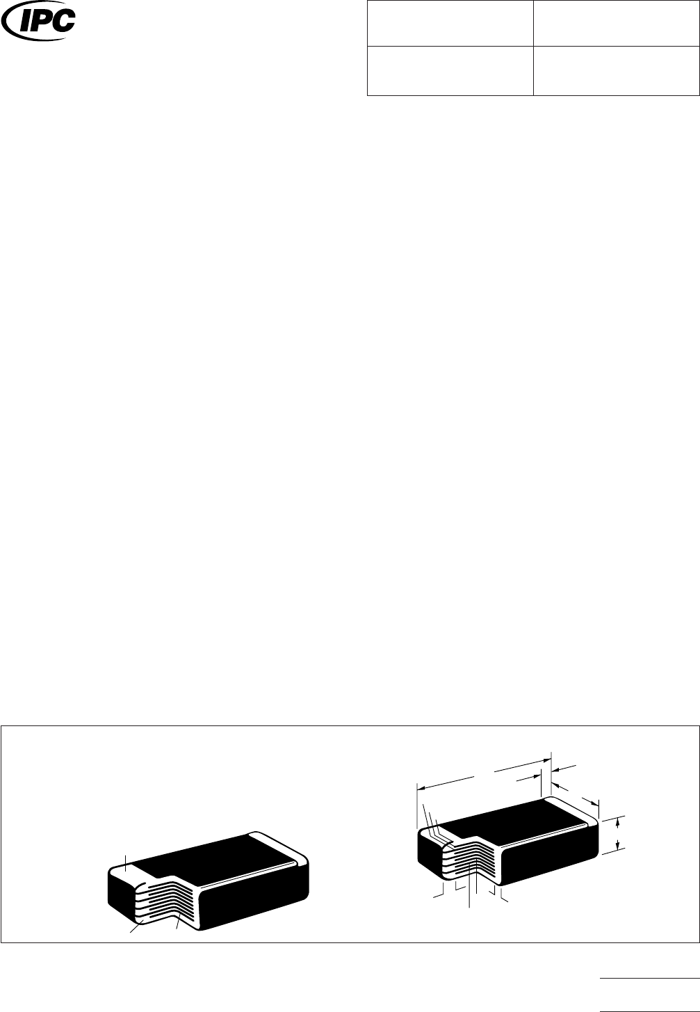
3.1 Basic Construction Multilayer ceramic capacitors use
substrate materials such as alumina for hybrid circuits and
porcelainized metal. The monolithic construction used in pro-
ducing these chips results in a solid block of ceramic with an
enclosed electrode system and metallized ends for circuit
attachment. This solid block is rugged and capable of with-
standing the harsh environment and treatment associated
with manufacturing processes. See Figure 1.
Electrodes are given a common terminal by coating the chip
ends with a precious metal-glass formulation suspended in an
organic vehicle. Consecutive drying and firing eliminates the
organic components and effects a bond between the ceramic
dielectric and glass constituent in the termination.
3.1.1 Termination Materials End terminations should be
solder coated with a tin/lead alloy. The solder should contain
between 58 to 68% tin. Solder may be applied to the termi-
nation by hot dipping or by plating from solution. Plated sol-
der terminations should be subjected to a post-plating reflow
operation to fuse the solder. The tin/lead finish should be at
least 0.0075 mm [0.0003 in] thick.
The termination shall be symmetrical, and shall not have nod-
ules lumps, protrusions, etc., that compromise the symmetry
or dimensional tolerances of the part. The end termination
shall cover the ends of the components, and shall extend out
to the top and bottom of the component.
Most common termination materials include palladium-silver
alloy, silver, and gold. Solder finish applied over precious
metal electrodes shall have a diffusion-barrier layer between
the electrode metallization and the solder finish. The barrier
layer should be nickel or an equivalent diffusion barrier, and
should be at least 0.00125 mm [0.00005 in] thick.
3.1.2 Marking Ceramic capacitors are typically unmarked.
3.1.3 Carrier Package Format Bulk rods, 8 mm tape/4
mm pitch is preferred for best handling. Tape and reel speci-
fications provide additional requirements.
3.1.4 Resistance to Soldering Parts should be capable of
withstanding five cycles through a standard reflow system
operating at 215°C. Each cycle shall consist of 60 seconds
exposure at 215°C. Parts must also be capable of withstanding a
minimum of 10 seconds immersion in molten solder at 260°C.
Caution should be exercised when using the 4564 (1825)
capacitor mounted on organic substrates due to CTE mis-
match if the assembly sees wide temperature swings in the
assembly process or end use.
IPC-782-8-2-1
Figure 1 Chip capacitor construction
1. Termination
2. Dielectric
3. Electrode
4. Chip length
5."A" electrode print
6. Electrode print
7. Cap (Topping layer)
8. End margin
9. Base layer
10. Shim (Active dielectric layer)
11. Side margin
12. Chip thickness
13. Chip width
14. Termination width
1
2 3
5
6
7
8
9
10
11
4
14
13
12
IPC-SM-782
Surface Mount Design
and Land Pattern Standard
Date
5/96
Section
8.2
Revision
A
Subject
Chip Capacitors
Page1of4
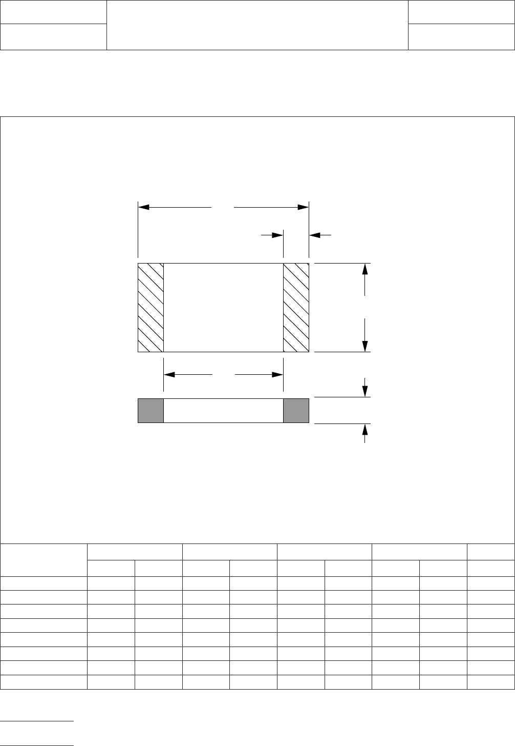
4.0 COMPONENT DIMENSIONS
Figure 2 provides the component dimensions for chip capacitors.
Component
Identifier
(mm) [in]
LSWTH
min max min max min max min max max
1005 [0402] 0.90 1.10 0.30 0.65 0.40 0.60 0.10 0.30 0.60
1310 [0504] 1.02 1.32 0.26 0.72 0.77 1.27 0.13 0.38 1.02
1608 [0603] 1.45 1.75 0.45 0.97 0.65 0.95 0.20 0.50 0.85
2012 [0805] 1.80 2.20 0.30 1.11 1.05 1.45 0.25 0.75 1.10
3216 [1206] 3.00 3.40 1.50 2.31 1.40 1.80 0.25 0.75 1.35
3225 [1210] 3.00 3.40 1.50 2.31 2.30 2.70 0.25 0.75 1.35
4532 [1812] 4.20 4.80 2.30 3.46 3.00 3.40 0.25 0.95 1.35
4564 [1825] 4.20 4.80 2.30 3.46 6.00 6.80 0.25 0.95 1.10
Figure 2 Chip capacitor component dimensions
L
S
T
W
H
IPC-782-8-2-2
IPC-SM-782
Subject
Chip Capacitors
Date
5/96
Section
8.2
Revision
A
Page2of4
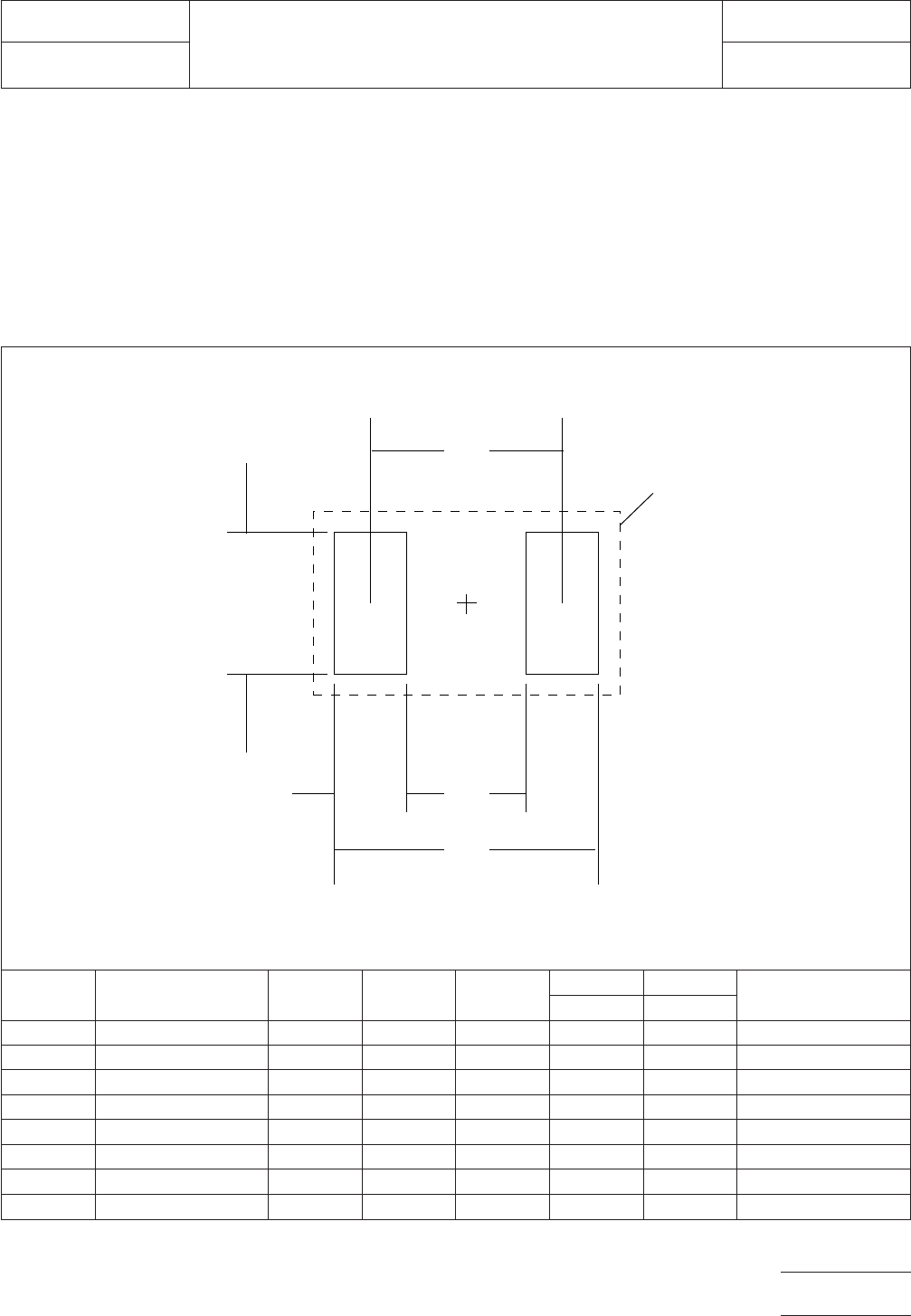
5.0 LAND PATTERN DIMENSIONS
Figure 3 provides the land pattern dimensions for chip capaci-
tors. These numbers represent industry consensus on the
best dimensions based on empirical knowledge of fabricated
land patterns.
In the table, the dimensions shown are at maximum material
condition (MMC). The least material condition (LMC) should
not exceed the fabrication (F) allowance shown on page 4.
The LMC and the MMC provide the limits for each dimension.
The dotted line in Figure 3 shows the grid placement court-
yard which is the area required to place land patterns and
their respective components in adjacent proximity without
interference or shorting. Numbers in the table represent the
number of grid elements (each element is 0.5 by 0.5 mm) in
accordance with the international grid detailed in IEC publica-
tion 97.
RLP No.
Component Identifier
(mm) [in] Z (mm) G (mm) X (mm)
YC
Placement Grid
(No. of Grid elements)ref ref
130A 1005 [0402] 2.20 0.40 0.70 0.90 1.30 2x6
131A 1310 [0504] 2.40 0.40 1.30 1.00 1.40 4x6
132A 1608 [0603] 2.80 0.60 1.00 1.10 1.70 4x6
133A 2012 [0805] 3.20 0.60 1.50 1.30 1.90 4x8
134A 3216 [1206] 4.40 1.20 1.80 1.60 2.80 4x10
135A 3225 [1210] 4.40 1.20 2.70 1.60 2.80 6x10
136A 4532 [1812] 5.80 2.00 3.40 1.90 3.90 8x12
137A 4564 [1825] 5.80 2.00 6.80 1.90 3.90 14x12
Figure 3 Chip capacitor land pattern dimensions
▼
▼
▼
▼
▼
▼
▼
▼
▼
C
G
Z
X
Y
Grid
placement
courtyard
▼
IPC-782-8-2-3
IPC-SM-782
Subject
Chip Capacitors
Date
5/96
Section
8.2
Revision
A
Page3of4