IPC-SM-782A-表面贴装焊盘图形设计标准.pdf.pdf - 第168页
4.0 COMPONENT DIMENSIONS Figure 2 provides the component dimensions for CQFP components. Component Identifier L (mm) S (mm) W (mm) T (mm) A (mm) B (mm) H (mm) P (mm) min max min max min max min max min max min max max bas…
1.0 SCOPE
This subsection provides the component and land pattern
dimensions for ceramic quad flat pack (CQFP) components.
Basic construction of the CQFP device is also covered. At the
end of this subsection is a listing of the tolerances and target
solder joint dimensions used to arrive at the land pattern
dimensions.
2.0 APPLICABLE DOCUMENTS
JEDEC Publication 95
Registered and Standard Outlines for
Solid JEDEC Publication 95 State and Related Products, Out-
line MS 044
3.0 COMPONENT DESCRIPTIONS
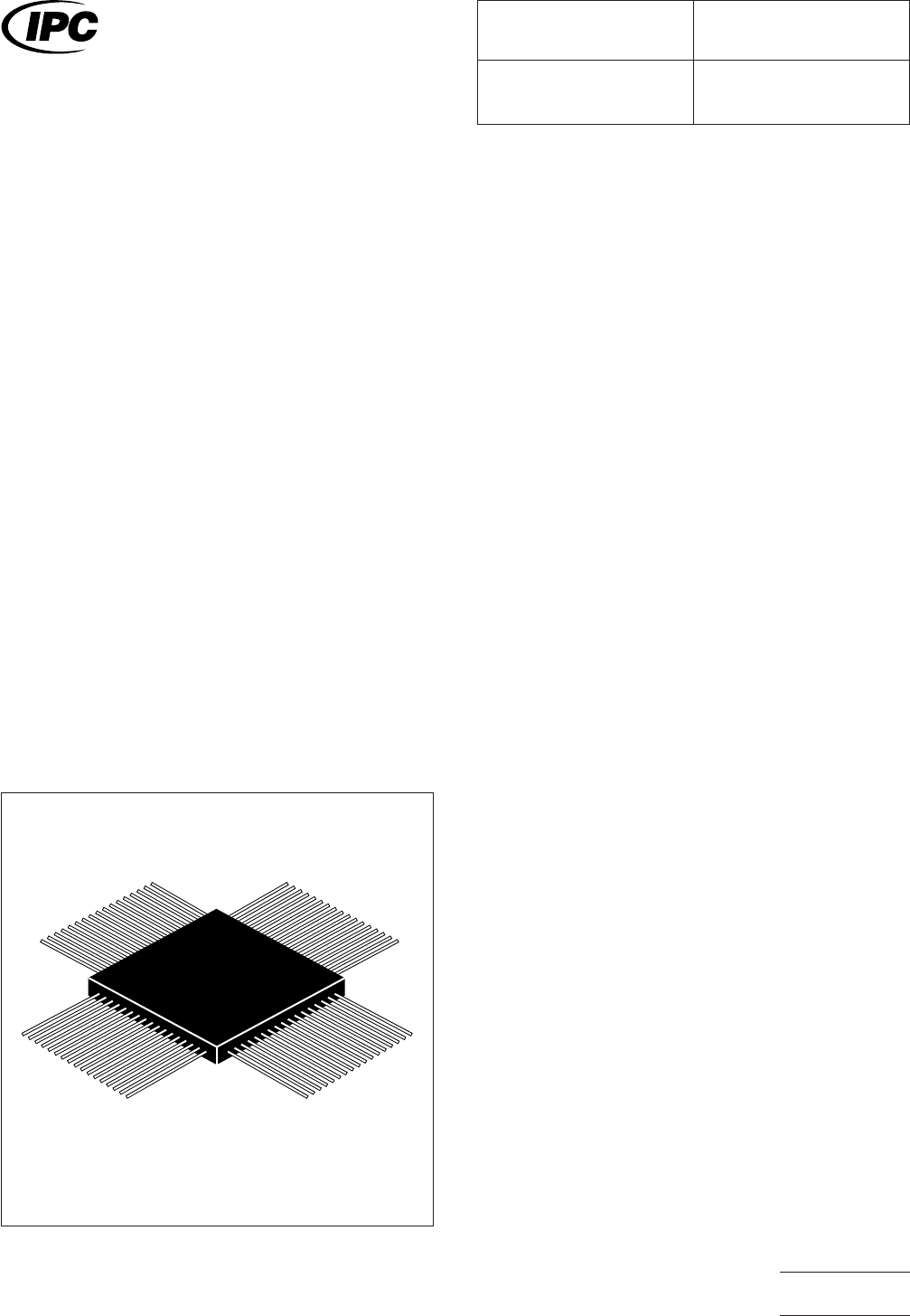
3.1 Basic Construction
See Figure 1. Leaded ceramic
chip carriers are typically supplied with an open cavity for chip
placement. Ceramic or metal lids are soldered, epoxied, or
attached with glass frit around the cavity to provide a hermetic
seal.
An exception to this construction is the JEDEC standard
MS044, which has the chip bonded to a lead frame, which is
then sealed between two ceramic bodies with glass frit, simi-
lar to CERDIP fabrication. The ceramic packages are available
in 28- through 196-lead configurations, with 1.27, 0.80, and
0.64 mm center spacing.
Pre-leaded ceramic chip carriers typically have copper alloy or
Kovar leads that are attached by the manufacturer. Leads are
typically bonded to metallization on the top surface of the chip
carrier. However, leads can be attached to the package cas-
tellations as well. Brazing or thermocompression bonding is
usually the attachment means.
Pre-leaded packages using lead-frame construction are also
available. These chip carriers have ceramic bodies with two
opposing halves which mate above and below a lead frame to
which the chip has been previously bonded. The seal is pre-
formed with glass frit.
Leads can be formed to different shapes, such as ‘‘J,’’ ‘‘L,’’
or ‘‘C’’ configurations. Leads bent in the ‘‘L’’ configuration are
known as ‘‘gullwings.’’
Pre-leaded chip carriers may be supplied with leads straight
and attached to a common strip. The user must detach the
common strip and form the leads to the desired configuration.
This is done to minimize lead bending during shipping and
handling. Leads may be supplied pre-tinned or with gold plat-
ing, as is often done for packages intended for a high reliabil-
ity user.
3.1.1 Termination Materials Leads must be solder-
coated with a tin/lead alloy. The solder should contain
between 58 to 68% tin. Solder may be applied to the leads by
hot dipping or by plating from solution. Plated solder termina-
tions should be subjected to post-plating reflow operation to
fuse the solder. The tin/lead finish should be at least 0.0075
mm [0.0003 in] thick.
3.1.2 Marking All parts shall be marked with a part number
and ‘‘Pin 1’’ location. Pin 1 location may be molded into the
plastic body.
3.1.3 Carrier Package Format Tube carriers are preferred
for best handling.
3.1.4 Process Considerations CQFPs are usually pro-
cessed using standard solder reflow processes. Parts should
be capable of withstanding ten cycles through a standard
reflow system operating at 215°C. Each cycle shall consist of
60 seconds exposure at 215°C.
IPC-782-11-4-1
CQFP construction
IPC-SM-782
Surface Mount Design
and Land Pattern Standard
Date
5/96
Section
11.4
Revision
A
Subject
CQFP
Page1of4
4.0 COMPONENT DIMENSIONS
Figure 2 provides the component dimensions for CQFP components.
Component
Identifier
L (mm) S (mm) W (mm) T (mm) A (mm) B (mm)
H
(mm)
P
(mm)
min max min max min max min max min max min max max basic
CQFP-28 14.40 14.80 11.86 12.39 0.32 0.48 1.02 1.27 9.05 10.05 9.05 10.05 2.30 1.270
CQFP-36 17.15 17.39 14.61 15.04 0.20 0.33 1.02 1.27 11.69 12.70 11.69 12.70 4.92 1.270
CQFP-44 19.69 19.93 17.15 17.58 0.20 0.33 1.02 1.27 14.23 15.24 14.23 15.24 4.92 1.270
CQFP-52 22.23 22.47 19.69 20.12 0.20 0.33 1.02 1.27 16.77 17.78 16.77 17.78 4.92 1.270
CQFP-68 27.31 27.55 24.77 25.20 0.20 0.33 1.02 1.27 21.85 22.86 21.85 22.86 4.92 1.270
CQFP-84 32.39 32.63 29.85 30.28 0.20 0.33 1.02 1.27 26.93 27.94 26.93 27.94 4.92 1.270
CQFP-100 37.47 37.71 34.93 35.36 0.20 0.33 1.02 1.27 32.01 33.02 32.01 33.02 4.92 1.270
CQFP-120 30.95 31.45 28.75 29.50 0.30 0.46 0.70 1.10 26.80 27.30 26.80 27.30 4.06 0.800
CQFP-128 30.95 31.45 28.75 29.50 0.30 0.46 0.70 1.10 26.80 27.30 26.80 27.30 4.06 0.800
CQFP-132 27.28 27.58 25.08 25.72 0.15 0.38 0.70 1.10 23.75 24.38 23.75 24.38 3.55 0.635
CQFP-144 30.95 31.45 28.75 29.50 0.30 0.46 0.70 1.10 26.80 27.30 26.80 27.30 4.06 0.800
CQFP-148 33.50 34.00 30.96 31.57 0.12 0.25 1.02 1.27 28.21 28.71 28.21 28.71 3.10 0.635
CQFP-160 30.95 31.45 28.75 29.50 0.30 0.46 0.70 1.10 26.80 27.30 26.80 27.30 4.06 0.800
CQFP-164 33.50 34.00 30.96 31.57 0.12 0.25 1.02 1.27 28.80 29.30 28.80 29.30 3.35 0.635
CQFP-196 35.75 36.25 33.21 33.82 0.12 0.25 1.02 1.27 33.80 34.30 33.80 34.30 3.45 0.635
Figure 2 CQFP component dimensions
Pin #1
indicator
[1]
▼
▼
E
▼
▼
▼
▼
W
Before trim & form
Pin #1
indicator
▼
▼
A
B
After trim & form
L
ST
H
▼
▼
▼
▼
▼
▼
▼
▼
▼
▼
▼
▼
▼
▼
▼
▼
2.5
MIN
T
0.25
MIN
Lead form detail
The industry standard for the ceramic quad flat pack device family is not well defined.
The above details represent several configurations considered common but other sizes are available
▼
IPC-782-11-4-2
IPC-SM-782
Subject
CQFP
Date
5/96
Section
11.4
Revision
A
Page2of4
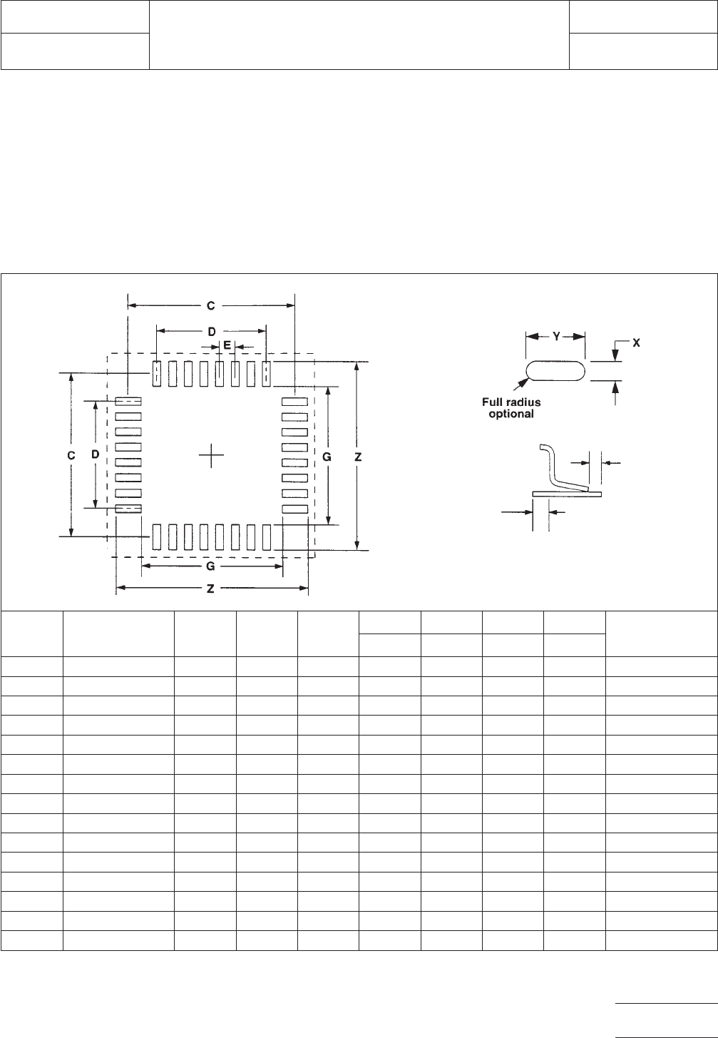
5.0 LAND PATTERN DIMENSIONS
Figure 3 provides the land pattern dimensions for CQFP com-
ponents. These numbers represent industry consensus on the
best dimensions based on empirical knowledge of fabricated
land patterns.
In the table, the dimensions shown are at maximum material
condition (MMC). The least material condition (LMC) should
not exceed the fabrication (F) allowance shown on page 4.
The LMC and the MMC provide the limits for each dimension.
The dotted line in Figure 3 shows the grid placement court-
yard which is the area required to place land patterns and
their respective components in adjacent proximity without
interference or shorting. Numbers in the table represent the
number of grid elements (each element is 0.5 by 0.5 mm) in
accordance with the international grid detailed in IEC publica-
tion 97.
RLP No.
Component
Identifier Z (mm) G (mm) X (mm)
Y (mm) C (mm) D (mm) E (mm)
Placement Grid
(No. of Grid
Elements)ref ref ref ref
750A CQFP-28 15.80 10.60 0.65 2.60 13.20 7.62 1.27 34x34
751A CQFP-36 18.60 13.80 0.65 2.40 16.20 10.16 1.27 40x40
752A CQFP-44 21.00 16.20 0.65 2.40 18.60 12.70 1.27 44x44
753A CQFP-52 23.60 18.80 0.65 2.40 21.20 15.24 1.27 50x50
754A CQFP-68 28.60 23.80 0.65 2.40 26.20 20.32 1.27 62x62
755A CQFP-84 33.80 29.00 0.65 2.40 31.40 25.40 1.27 70x70
756A CQFP-100 38.80 34.00 0.65 2.40 36.40 30.48 1.27 80x80
757A CQFP-120 32.40 28.00 0.50 2.20 30.20 23.20 0.80 68x68
758A CQFP-128 32.40 28.00 0.50 2.20 30.20 24.80 0.80 68x68
759A CQFP-132 28.60 24.20 0.40 2.20 26.40 20.32 0.64 60x60
760A CQFP-144 32.40 28.00 0.50 2.20 30.20 24.80 0.80 68x68
761A CQFP-148 35.20 30.00 0.35 2.60 32.60 22.86 0.64 72x72
762A CQFP-160 32.40 28.00 0.50 2.20 30.20 24.80 0.80 68x68
763A CQFP-164 35.20 30.00 0.35 2.60 32.60 25.40 0.64 72x72
764A CQFP-196 37.20 32.00 0.35 2.60 34.60 30.48 0.64 76x76
Figure 3 CQFP land pattern dimensions
IPC-782-11-4-3
IPC-SM-782
Subject
CQFP
Date
5/96
Section
11.4
Revision
A
Page3of4