IPC-SM-782A-表面贴装焊盘图形设计标准.pdf.pdf - 第27页
3.5.3 Service Life The design service life, N, can vary significantly for the use categories in T able 3–6. The design service lives can range from less than one year , barely exceeding the warranty period for consumer pr…

assembly process options outlined. Product size, compo-
nent types, projected volume and the level of manufactur-
ing equipment available may affect process options.
Following the substrate development, the assembly will be
evaluated for many of the fundamentals necessary to insure
a successful SMT process. Specific areas addressed during
the evaluation will include:
• Land pattern concepts
• Component selection
• Mounting substrate design
• Need for testability
• Phototool generation
3.4.1 SMT Land Pattern The use of process proven land
patterns for the solder attachment of surface mount devices
will provide a benchmark to evaluate solder joint quality.
Land pattern geometry and spacing utilized for each com-
ponent type must accommodate all physical variables
including size, material, lead contact design and plating.
3.4.2 Standard Component Selection Whenever pos-
sible, SMT devices should be selected from standard con-
figurations. The standard components will be available
from multiple sources and will usually be compatible with
all assembly processes. For those devices developed to
meet specific applications, standard packaging is often
available. Select a package type that will be similar in
materials and plating of standard device types when pos-
sible.
3.4.3 Circuit Substrate Development Design the circuit
substrate to minimize excessive costs. Surface Mount Tech-
nology often pushes the leading edge of substrate technol-
ogy. When estimating circuit density, allow for the greatest
latitude in fabrication processes and tolerance variables.
Before adopting extreme fine line and utilizing small plated
holes, understand the cost impact, yield, and long-term reli-
ability of the product.
3.4.4 Assembly Considerations Other factors that will
impact manufacturing efficiency include component place-
ment. Maintaining a consistent spacing between compo-
nents, common orientation or direction of polarized devices
will impact all steps of the assembly process. In addition,
when common orientation is maintained, machine pro-
gramming is simplified and component verification, solder
inspection and repair are simplified.
3.4.5 Provide for Automated Test Testability of the
assembled circuit substrate must be planned well in
advance. If component level testing is necessary, one test
probe contact area is required for each common node or
net. Ideally, all probe contact pads are on one side. Provide
grid-based test nodes to accommodate standard probes.
Functional testing may also employ the same test nodes
used for in-circuit test but will include all connectors that
interface to cables and other assemblies.
3.4.6 Documentation for SMT Documentation used to
fabricate the circuit substrate and assemble the product
must be accurate and easy to understand. Details, specifi-
cations and notes will guide both the assembly processing
and control the quality level of a product. Unique materials
or special assembly instructions should be included on the
face of the detail drawings or included in the documenta-
tion package.
3.5 Environmental Constraints
3.5.1 Handling Moisture Sensitive Components
Sev-
eral large plastic packages may be susceptible to absorbing
moisture. The component manufacturer usually packages
these parts with a desiccant, and provides instruction for
use or maintaining those parts in a controlled storage envi-
ronment. See J-STD-020 and J-STD-033 for instructions
and proper handling and tesing procedures.
3.5.2 Usage Environments In Table 3–6, worst-case, but
realistic, use environments for SM electronic assemblies
are shown in nine major use categories. These use environ-
ment categories are listed in order of increasing severity,
without consideration of the number of expected service
years. It should be noted that the cyclic temperature range,
delta T, is not the difference between the possible mini-
mum, Tmin, and maximum, Tmax, operational temperature
extremes; delta T is significantly less. It has to be recog-
nized that these temperature extremes are possible only
during different times of the year, and then only at signifi-
cantly different geographic locations. The delta T values
represent the temperature swings that typically can be
expected during a given operating cycle.
Also given are the expected dwell durations at operating
temperatures; they are significant because they determine
the degree of completeness of the stress relaxation in the
solder joints and thus determine the amount of cyclic
fatigue damage relative to the maximum fatigue damage at
complete stress relaxation. Table 3–6 also gives estimates
of the number of operating cycles occurring during a ser-
vice year. For some of the use categories, the use environ-
ments are described in terms of the sum of multiple use
environments resulting from either significant seasonal
dependence or broadly foreseeable use conditions; the mili-
tary avionics category is subdivided into three subcatego-
ries reflecting differing use conditions due to type of air-
craft, mission profile, geographic effects, etc. The space
category contains two different environments for satellites
in low-earth orbit (LEO) or geo-synchronous (stationary
relative to earth) orbit (GEO).
IPC-SM-782A December 1999
18
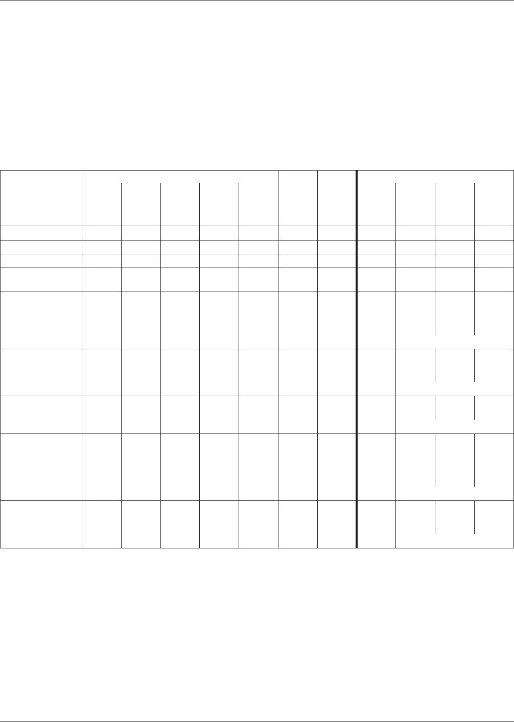
3.5.3 Service Life The design service life, N, can vary
significantly for the use categories in Table 3–6. The design
service lives can range from less than one year, barely
exceeding the warranty period for consumer products, to
20 years or more for telecommunications equipment and
commercial aircraft. For some military applications the ser-
vice life is measured in thousands of hours.
3.5.4 Acceptable Cumulative Failure Probability The
acceptable cumulative failure probability, F(N), at the end
of the design service life, N, can vary significantly depend-
ing on the specific purpose of the product, the complexity
(number and mix of components) of the product, and per-
haps the design service life. F(N) values could range from
1 ppm for products whose failure has critical conse-
quences, e.g., cardiac pacemakers, to perhaps 10,000 ppm
(1%) for consumer products or products which provide
redundancy or ‘‘limp-home capability’’ in case of electrical
system failure. (See IPC-SM-785).
Table 3–6 Worst-Case Environments and Appropriate Equivalent Accelerated Testing
USE CATEGORY
WORST-CASE USE ENVIRONMENT ACCELERATED TESTING
Tmin
°C
Tmax
°C
∆T
(1)
°C
t
D
hrs
Cycles/
year
Typical
Years
of
Service
Approx.
Accept.
Failure
Risk, %
Tmin
°C
Tmax
°C
∆T
(2)
°C
t
D
min
1) CONSUMER 0 +60 35 12 365 1-3 1 +25 +100 75 15
2) COMPUTERS +15 +60 20 2 1460 5 0.1 +25 +100 75 15
3) TELECOM - 40 +85 35 12 365 7-20 0.01 0 +100 100 15
4) COMMERCIAL
AIRCRAFT
-55 +95 20 12 365 20 0.001 0 +100 100 15
5) INDUSTRIAL &
AUTOMOTIVE
PASSENGER
COMPARTMENT
-55 +95 20
&40
&60
&80
12
12
12
12
185
100
60
20
10 0.1 0 +100 100 15
& COLD
(3)
6) MILITARY
GROUND &
SHIP
-55 +95 40
&60
12
12
100
265
10 0.1 0 +100 100 15
& COLD
(3)
7) SPACE leo
geo
-55 +95 3
to 100
1
12
8760
365
5-30 0.001 0 +100 100 15
& COLD
(3)
8) MILITARY
AVIONICS a
b
c
-55 +95 40
60
80
&20
2
2
2
1
365
365
365
365
10 0.01 0 +100 100 15
& COLD
(3)
9) AUTOMOTIVE
UNDER HOOD
-55 +125 60
&100
&140
1
1
2
1000
300
40
5 0.1 0 +100 100 15
& COLD
(3)
& LARGE ∆T
(4)
& = in addition
1) ∆T represents the maximum temperature swing, but does not include power dissipation effects; for power dissipation calculate ∆T;
power dissipation can make pure temperature cycling accelerated testing significantly inaccurate. It should be noted that the cyclic
temperature range, ∆T, is not the difference between the possible minimum, T
MIN
, and maximum, T
MAX
, operational temperature
extremes; ∆T is typically significantly less.
2) All accelerated test cycles shall have temperature ramps <20°C/minute and dwell times at temperature extremes shall be 15 min-
utes measured on the test boards. This will give ~24 test cycles/day.
3) The failure/damage mechanism for solder changes at lower temperatures; for assemblies seeing significant cold environment
operations, additional ‘‘COLD’’ cycling, from perhaps –40 to 0°C, with dwell times long enough for temperature equilibration and for
a number of cycles equal to the ‘‘COLD’’ °C operational cycles in actual use is recommended.
4) The failure/damage mechanism for solder is different for large cyclic temperature swings traversing the stress-to-strain –20 to
+20°C transition region; for assemblies seeing such cycles in operation, additional appropriate ‘‘LARGE ∆T’’ testing with cycles
similar in nature and number to actual use is recommended.
December 1999 IPC-SM-782A
19
3.6 Design Rules During the component selection phase
of a design, manufacturing engineering should be consulted
regarding any components outside the scope of this docu-
ment.
The printed board design principles are a statement of cur-
rent test and manufacturing capabilities. Exceeding or
changing these capabilities requires concurrence of all par-
ticipants in the process including manufacturing, engineer-
ing and test technology.
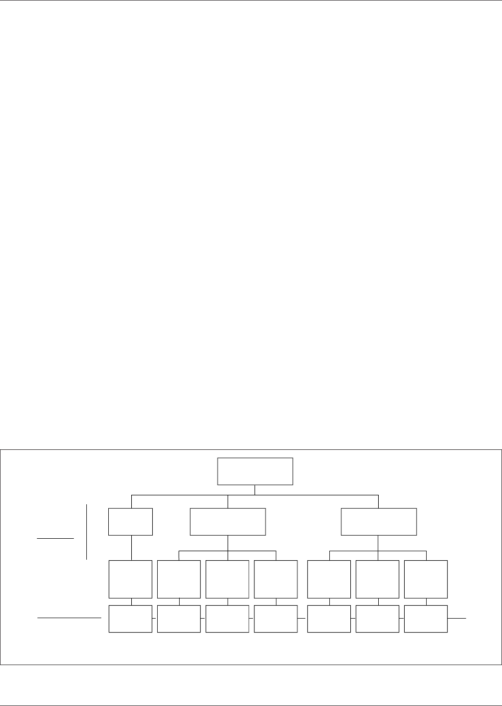
Involving test and manufacturing early in the design helps
to move a quality product quickly into production. Figure
3–7 shows a list of concurrent engineering team partici-
pants that should be involved.
3.6.1 Component Spacing
3.6.1.1 Component Considerations
The land pattern
design information discussed so far is important for reli-
ability of surface mount assemblies. However, the designer
should not lose sight of manufacturability, testability and
repairability of SMT assemblies. A minimum interpackage
spacing is required to satisfy all these manufacturing
requirements. There is no limit on maximum interpackage
spacing; the more the better. Some designs require that sur-
face mount components are positioned as tightly as pos-
sible. Based on experience, the examples shown in Figure
3–8 meet manufacturability requirements.
The land to land spacing between adjacent components
should be 1.25 mm [0.050 in] clear space all around the
edges of printed boards if boards are tested off the connec-
tor or 2.5 mm [0.100 in] minimum if vacuum seal for test-
ing is used. The requirements specified herein are recom-
mended minimums excluding conductor geometry
tolerances.
3.6.1.2 Wave Solder Component Orientation All polar-
ized surface mount components should be placed in the
same orientation, when possible. On any printed board
assembly where the secondary side is to be wave soldered,
the preferred orientation of devices on that side is
described and shown in Figure 3–9. The preferred orienta-
tion is used in order to optimize the resulting solder joint
quality as the assembly exits the solder wave.
• All passive components shall be parallel to each other.
• All SOICs shall be perpendicular to the long axis of
passive components.
• The longer axis of SOICs and of passive components
shall be perpendicular to each other.
• The long axis of passive components shall be perpen-
dicular to the direction of travel of the board along
the conveyer of the wave solder machine.
3.6.1.3 Component Placement Similar types of compo-
nents should be aligned on the board in the same orienta-
tion for ease of component placement, inspection, and sol-
dering. Also, similar component types should be grouped
together whenever possible, with the net list or connectiv-
ity and circuit performance requirements ultimately driving
the placements. See Figure 3-10. In memory boards, for
example, all of the memory chips are placed in a clearly
defined matrix with pin one orientation the same direction
for all components. This is a good design practice to carry
out on logic designs where there are many similar compo-
nent types with different logic functions in each package.
On the other hand, analog designs often require a large
variety of component types making it understandably diffi-
cult to group similar components together. Regardless if
IPC-782-3-7
Figure 3–7 Simplified electronic development organization
▼
▼
▼
▼
▼
▼
▼
▼
▼
Admin-
istrative
control
Chain of
command
Operational
control
Working
level
PROGRAM
OFFICE
System
Manage-
ment
Project
Task
MANAGEMENT
ENGINEERING
MANAGEMENT
System
Engin-
eering
Elec-
tronic
Design
MANUFACTURING
MANAGEMENT
Product
Design
Fabri-
cation
Assem-
bly
Testing
Project
Task
Project
Task
Project
Task
Project
Task
Project
Task
Project
Task
Deliverable
Hardware
IPC-SM-782A December 1999
20