IPC-SM-782A-表面贴装焊盘图形设计标准.pdf.pdf - 第190页
6.0 TOLERANCE AND SOLDER JOINT ANALYSIS Figure 4 provides an analysis of tolerance assumptions and resultant solder joints based on the land pattern dimensions shown in Figure 3. Tolerances for the component dimensions, …
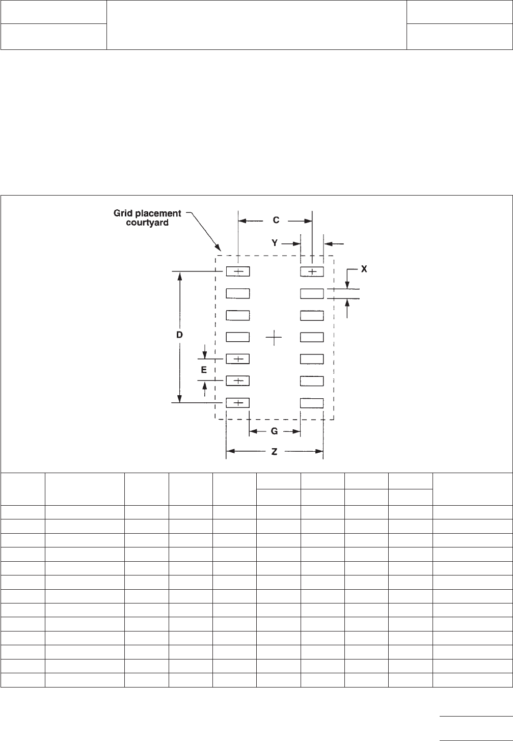
5.0 LAND PATTERN DIMENSIONS
Figure 3 provides the land pattern dimensions for DIP compo-
nents. These numbers represent industry consensus on the
best dimensions based on empirical knowledge of fabricated
land patterns.
In the table, the dimensions shown are at maximum material
condition (MMC). The least material condition (LMC) should
not exceed the fabrication (F) allowance shown on page 4.
The LMC and the MMC provide the limits for each dimension.
The dotted line in Figure 3 shows the grid placement court-
yard which is the area required to place land patterns and
their respective components in adjacent proximity without
interference or shorting. Numbers in the table represent the
number of grid elements (each element is 0.5 by 0.5 mm) in
accordance with the international grid detailed in IEC publica-
tion 97.
RLP No.
Component
Identifier Z (mm) G (mm) X (mm)
Y (mm) C (mm) D (mm) E (mm)
Placement Grid
(No. of Grid
Elements)ref ref ref ref
860 DIP 8 9.80 5.40 1.20 2.20 7.60 7.62 2.54 22x24
861 DIP 14 9.80 5.40 1.20 2.20 7.60 15.24 2.54 22x42
862 DIP 16 9.80 5.40 1.20 2.20 7.60 17.78 2.54 22x44
863 DIP 18 9.80 5.40 1.20 2.20 7.60 20.32 2.54 22x48
864 DIP 20 9.80 5.40 1.20 2.20 7.60 22.86 2.54 22x56
865 DIP 22L 12.40 8.00 1.20 2.20 10.20 25.40 2.54 26x58
866 DIP 24 9.80 5.40 1.20 2.20 7.60 27.94 2.54 38x66
867 DIP 24L 12.40 8.00 1.20 2.20 10.20 27.94 2.54 26x64
867 DIP 24X 17.40 13.00 1.20 2.20 15.20 27.94 2.54 36x68
869 DIP 28 9.80 5.40 1.20 2.20 7.60 33.02 2.54 22x74
870 DIP 28X 17.40 13.00 1.20 2.20 15.20 33.02 2.54 36x84
871 DIP 40X 17.40 13.00 1.20 2.20 15.20 48.26 2.54 36x110
872 DIP 48X 17.40 13.00 1.20 2.20 15.20 58.42 2.54 36x130
Figure 3 DIP land pattern dimensions
IPC-782-13-1-3
IPC-SM-782
Subject
DIP
Date
8/93
Section
13.1
Revision
Page3of4
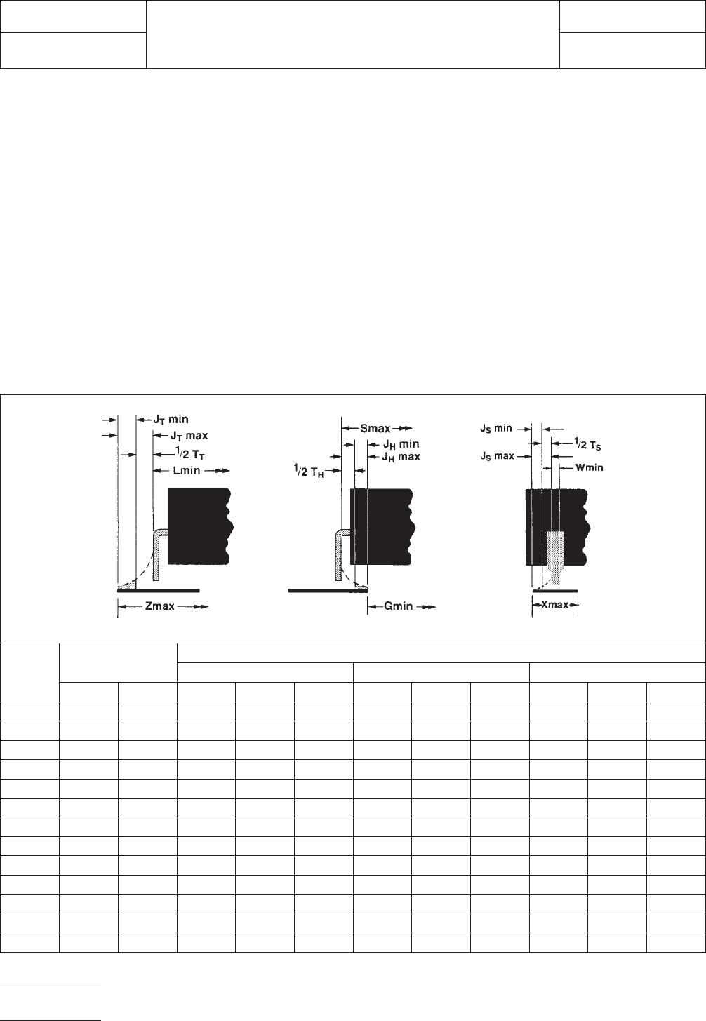
6.0 TOLERANCE AND SOLDER JOINT ANALYSIS
Figure 4 provides an analysis of tolerance assumptions and
resultant solder joints based on the land pattern dimensions
shown in Figure 3. Tolerances for the component dimensions,
the land pattern dimensions (fabrication tolerances on the
interconnecting substrate), and the component placement
equipment accuracy are all taken into consideration.
Figure 4 provides the solder joint minimums for toe, heel, and
side fillets, as discussed in Section 3.3. The tolerances are
addressed in a statistical mode, and assume even distribution
of the tolerances for component, fabrication, and placement
accuracy.
Individual tolerances for fabrication (‘‘F’’) and component
placement equipment accuracy (‘‘P’’) are assumed to be as
given in the table. These numbers may be modified based on
user equipment capability or fabrication criteria. Component
tolerance ranges (C
L
,C
S
, and C
W
) are derived by subtracting
minimum from maximum dimensions given in Figure 2. The
user may also modify these numbers, based on experience
with their suppliers. Modification of tolerances may result in
alternate land patterns (patterns with dimensions other than
the IPC registered land pattern dimensions).
The dimensions for minimum solder fillets at the toe, heel, or
side (J
T
,J
H
,J
S
) have been determined based on industry
empirical knowledge and reliability testing. Solder joint
strength is greatly determined by solder volume. An observ-
able solder fillet is necessary for evidence of proper wetting.
Thus, the values in the table usually provide for a positive sol-
der fillet. Nevertheless, the user may increase or decrease the
minimum value based on process capability.
RLP No.
Tolerance
Assumptions (mm)
Solder Joint
Toe (mm) Heel (mm) Side (mm)
FPC
L
J
T
min J
T
max C
S
J
H
min J
H
max C
W
J
S
min J
S
max
860 0.20 0.20 0.630 0.74 1.09 0.679 0.70 1.07 0.200 0.25 0.42
861 0.20 0.20 0.630 0.74 1.09 0.679 0.70 1.07 0.200 0.25 0.42
862 0.20 0.20 0.630 0.74 1.09 0.679 0.70 1.07 0.200 0.25 0.42
863 0.20 0.20 0.630 0.74 1.09 0.679 0.70 1.07 0.200 0.25 0.42
864 0.20 0.20 0.630 0.74 1.09 0.679 0.70 1.07 0.200 0.25 0.42
865 0.20 0.20 0.880 0.78 1.25 0.916 0.55 1.03 0.200 0.25 0.42
866 0.20 0.20 0.630 0.74 1.09 0.679 0.70 1.07 0.200 0.25 0.42
867 0.20 0.20 0.880 0.78 1.25 0.916 0.55 1.03 0.200 0.25 0.42
868 0.20 0.20 0.630 0.73 1.08 0.679 0.71 1.08 0.200 0.25 0.42
869 0.20 0.20 0.630 0.74 1.09 0.679 0.70 1.07 0.200 0.25 0.42
870 0.20 0.20 0.630 0.73 1.08 0.679 0.71 1.08 0.200 0.25 0.42
871 0.20 0.20 0.630 0.73 1.08 0.679 0.71 1.08 0.200 0.25 0.42
872 0.20 0.20 0.630 0.73 1.08 0.679 0.71 1.08 0.200 0.25 0.42
Figure 4 Tolerance and solder joint analysis
IPC-782-13-1-4
IPC-SM-782
Subject
DIP
Date
8/93
Section
13.1
Revision
Page4of4
1.0 INTRODUCTION
This section covers land pattern recommendations for ball
grid array (BGA) contact devices. Each subsection contains
information in accordance with the following format.
1.0 Scope
2.0 Applicable Documents
3.0 General Component Description
4.0 Component Outline
5.0 Land Pattern Dimensions
6.0 Land Pattern Analysis
The following is the table of contents for this section:
Table of Contents
Components with Ball Grid Array Contacts
Section
14.1
14.2
Family
PBGA
R-PBGA
2.0 APPLICABLE DOCUMENTS
The following documents, of the issue in effect on the current
revision date of this section, form a part of this specification to
the extent specified herein.
2.1 Electronic Industries Alliance (EIA) Automated Com-
ponent Handling (ACH) Convention
1
ACH:EIA-481-A Taping of Surface Mount Components for
Automated Placement.
ACH:EIA-481-3 32, 44 and 56 mm Embossed Carrier Tap-
ing of Surface Mount Components for Automated Handling.
2.2 Joint Electronic Device Engineering Council
2
JEDEC Publication 95 Registered and Standard Outlines for
Solid State and Related Products:
• Plastic Ball Grid Array (PBGA), MO-151 and MS-028
• Thick Matrix Tray for Handling/Shipping of Ball Grid Array
Packages, CO-028
• Thin Matrix Tray for Shipping and Handling of Ball Grid
Packages, CO-029.
2.3 Electronic Industries Association of Japan (EIAJ)
3
EIAJ-ED-7404 General Rules for the Preparation of Outline
Drawings of Integrated Circuits
2.4 International Electrotechnical Commission (IEC)
4
IEC-97 Requirements for Uniform Grid Elements
IEC-60191-2 Mechanical Standardization of Solid State
Products
2.5 Joint Industry Standards
5
J-STD-013 Implementation of Ball Grid Array and Other High
Density Technology
3.0 GENERAL INFORMATION
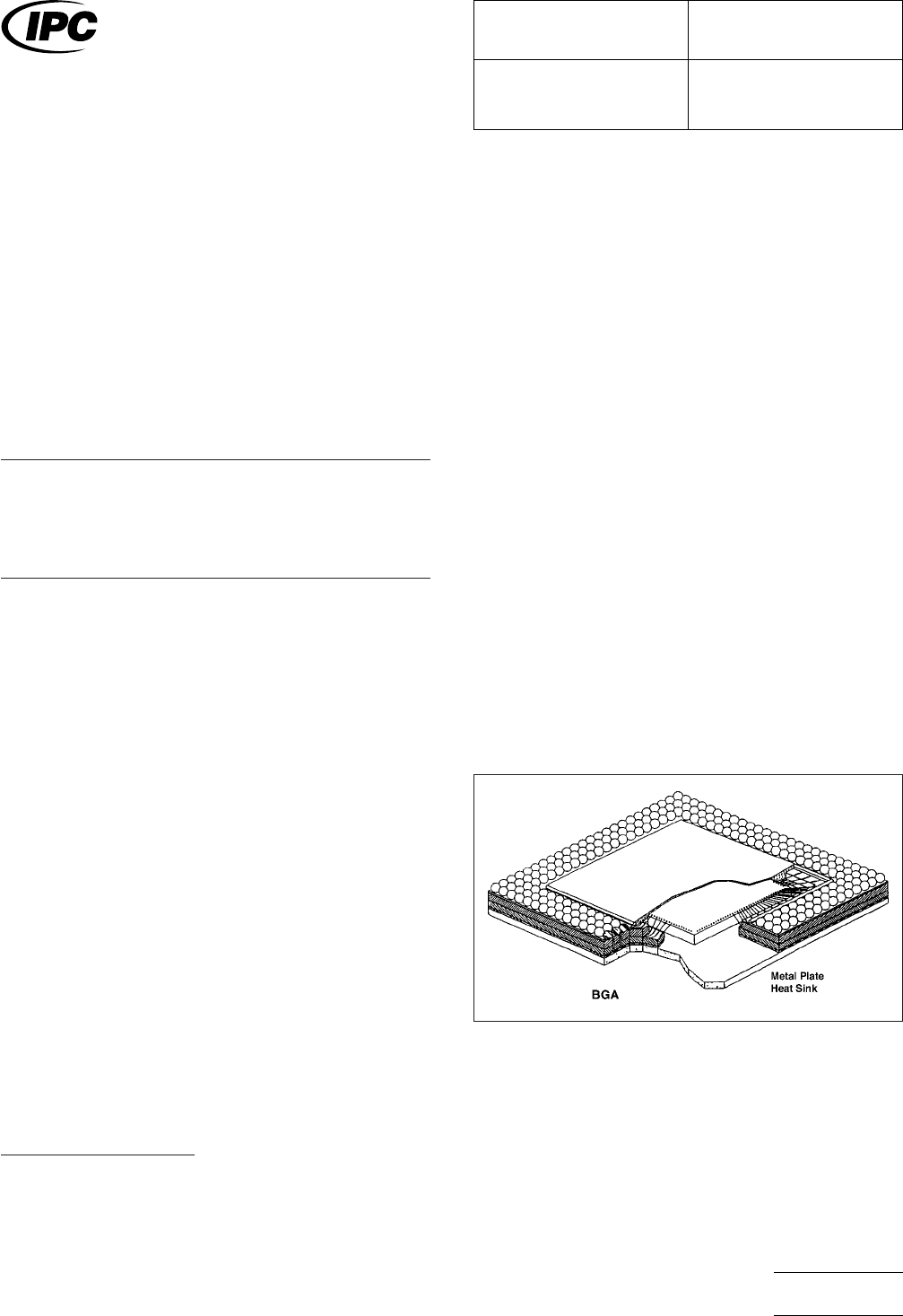
3.1 Component Description
The Grid Array device family
includes square and rectangular package configurations and
is furnished in a variety of base materials. Figure 3-1 shows
the elements of a BGA. Base material serves as a mounting
structure for attaching the die. Depending on the physical
characteristics of the material, flip-chip or wire bond technolo-
gies may be employed to route the signal from the die bond
pads to the array matrix on the base interface structure. Fig-
ure 3-2 compares the top surface attached die to the cavity
down configuration.
The interface contact or grid is arranged in a uniform column
and row format. The standard basic spacing or pitch for the
1. EIA: 2500 Wilson Blvd., Arlington, VA, 22201-3834, USA.
2. JEDEC: 2500 Wilson Blvd., Arlington, VA, 22201-3834, USA.
3. EIAJ: 8th Toyo Kaiji Building 6F, 1-5-13 Nishi-Shinbashi, Minato-ku Tokyo 105, Japan.
4. IEC: 3 rue de Verembe, PO Box 131-1211, Geneva 20, Switzerland.
5. IPC: 2215 Sanders Road, Northbrook, IL 60062
IPC-782143-1
Figure 3-1 Ball Grid Array IC package example
IPC-SM-782
Surface Mount Design
and Land Pattern Standard
Date
4/99
Section
14.0
Revision
—
Subject
Components with Ball
Grid Array Contacts
Page1of6