IPC-SM-782A-表面贴装焊盘图形设计标准.pdf.pdf - 第55页
The overall impact on SMT printed board real estate must be considered when designing for test. There are three cat- egories of design for test rules being employed on SMT designs: 1) complete the design, and add the tes…

change after the design is complete. A generic test philoso-
phy which has been applied to hundreds of dense SMT
designs successfully.
• Strategic placement of all component vias
• Provide access to every node of every net
• Access every node from both sides of the board
• Grid based component and via placement
• Correct test pad geometries and clearances
• Do not probe directly to SMT component lands
Even in the most dense designs, the philosophy of provid-
ing 100% access to every node of every net from either
side of the board can be accomplished. However, this deci-
sion must be made at the beginning of a design.
5.2.3 Test Strategy After the product test philosophy
has been established, a test strategy or procedure can be
defined. For an overview of several elements of a proce-
dure consider the following:
• Vision inspection of inner layers using AOI
• Vision inspection of O/L land/via connections
• Probe only vias on either side for bare board test
• Do not damage SMT lands with probe tips
• Probe secondary side vias for loaded test board
• Screen paste on vias for airtight board
The actual product test strategy must be organized by all of
the concurrent engineering team members who will be
involved in the testing process. This will insure that the
integration of the various test types and procedures will not
have too much redundancy, or create gaps which may
endanger test integrity.
5.2.4 Rework Strategy Rework of a multilayer SMT
printed board can be difficult or impossible due to limited
access to inner layer conductors. Typical rework proce-
dures consist of manually cutting an inner layer conductor
with special knives, programming a drill to move the board
to a site on the board and then drilling a controlled depth
hole to disconnect an inner layer conductor, or, lifting a
lead on a surface mount component.
In the case of densely populated SMT boards, certain com-
ponents may even have to be removed to gain access to a
site where an inner layer conductor is to be cut. This vio-
lates an important rule with SMT components: Do not
remove components from the board unless it is absolutely
necessary. Doing so weakens the bond strength of the land
to the board and may even cause the land to lift off the
board. With some designs, where grid based 100% test via
accessibility is built into the land pattern, the rework ports
have been created. Each test via provides access to every
conductor on every layer of the board without exception. In
order to remove any terminal of any device from a net, the
via may simply be drilled out by hand.
Using the vias as rework ports eliminates the need to
remove any components, drill extra holes in the board, or
cut into the board with a knife to disconnect nets.
Following disconnection, the device terminal may be
reconnected to another terminal by simply soldering a wire
to the terminal with a fine tip soldering iron. This is usu-
ally accomplished without disturbing any solder joints on
the board, including the lead that is being soldered to the
wire.
Aside from the wire, using this approach to rework an
SMT printed board leaves no visible indications or obvious
damage to highlight that the board has been modified.
5.3 Full Nodal Access Full nodal access has a different
meaning for the bare board test than for the ATE test. To
achieve full integrity at the bare board test level, 100%
access to every node of every net is required. The number
of test probes needed to test the board is equal to the total
number of device terminations. However, in the case of
most dense Surface Mount designs, this often requires the
use of a double sided, or clamshell test fixture because all
of the nodes are not accessible from one side of the board.
The ATE test only needs to have access to one node per
net. Every net has at least two nodes. Some nets have many
nodes, for example, on memory boards one net may be
connected to many nodes. In order to achieve full integrity
at the ATE test level, access to only one node of each net
is all that is required. Therefore, the total number of test
probes required to perform the ATE test is significantly less
than the number required for the bare board test.
There are two alternatives to building in testability to the
SMT printed board at the design phase. One is to build in
100% nodal access for the bare board test, with the second-
ary benefit being that 100% access for the loaded board test
is automatically built in.
The other alternative is to build in 100% nodal accessibil-
ity for the loaded board test during the design phase. This
approach will almost certainly guarantee that the bare
board test will not have sufficient grid based test nodes
available to complete the test without the use of a clam-
shell or two one-sided fixtures.
The use of design concepts with grid based 100% nodal
access from either side of the board is the most economical
approach from the total process perspective. If the grid
based test land concept is used, the test fixtures for bare
and loaded board tests will not become obsolete through
later board connectivity revisions. This is yet another sav-
ings downstream in the product development process. Also,
if the printed board uses buried vias, the grid based test
land concept with 100% nodal access will even provide
access to those buried nets from the ends of the nets. This
is another benefit realized during the bare board test.
IPC-SM-782A December 1999
46
The overall impact on SMT printed board real estate must
be considered when designing for test. There are three cat-
egories of design for test rules being employed on SMT
designs:
1) complete the design, and add the test nodes randomly at
the end;
2) develop land patterns with test vias on a 2.5 mm [0.100
in] grid;
3) develop land patterns with test vias on a 1.25 mm [0.050
in] grid.
The random approach needs no discussion. The second
approach of bringing the land pattern test vias to a 2.5 mm
[0.100 in] grid works with sparsely populated boards, but
this approach consumes almost as much real estate as using
Through Hole components. With the high component den-
sity requirements of most SMT designs, the third approach
of bringing the land pattern test vias to a 1.25 mm [0.050
in] grid is the only method which will allow 100% test
node accessibility for all printed board assembly types.
SMT has been and will continue to force the test grid down
to 1.25 from 2.5 mm [0.050 from 0.100 inch]. Fine pitch
components may force the test grid down to an even
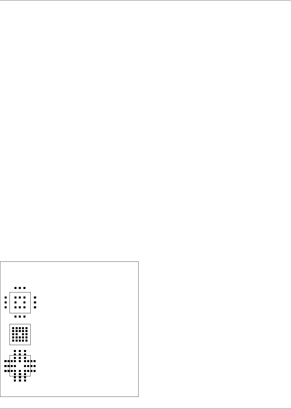
smaller size. Figure 5–1 is a schematic of various lead
pitch and test grid combinations. Using a 2.5 mm [0.100
inch] test grid on a 1.25 mm [0.050 inch] pitch component
consumes excessive real estate and is impossible on dense
SMT designs. A 1.25 mm [0.050 inch] test grid on a 1.25
mm [0.050 inch] pitch component yields the most eco-
nomical solution in terms of real estate and test node acces-
sibility. Furthermore, it can be seen that Fine Pitch compo-
nent land patterns can also be developed with the test vias
on a 1.25 mm [0.050 in] grid.
For fine pitch components it is good design practice to
bring approximately half of the test vias to the inside of the
land pattern and the other half to the outside of the land
pattern. This accomplishes two objectives: 1) the maximum
loading of 100 test points per square inch limitation of all
test equipment is not exceeded: and 2) wider distribution of
test points reduces the high pressure point areas which
cause fixture bowing during vacuum or mechanical actua-
tion.
5.3.1 In-Circuit Test Accommodation Specific via lands
and holes can be accessed for automatic in-circuit test
(ICT). The via land location for each common network in
a circuit is matched to a test probe contact in the test fix-
ture. The test system can then drive each device on the
assembly and quickly locate defective devices or identify
assembly process problems.
To insure precise alignment of the probe contact pins with
the printed board, exact probe position and specific net-
works must be furnished to the fixture developer. Identify-
ing the test locations as components in the CAD data base
will allow for easy transfer of drilling data. This data will
reduce fixture development time and eliminate the drilling
of excessive, non-functional holes in the fixture base.
5.4 Limited Nodal Access Limited nodal access (less
than 100%) still allows the use of ATE bed-of-nails testing,
but not as effectively as full nodal access does. As soon as
nodal access goes below 100%, shorts, defects and
in-circuit testing cannot be performed completely, and so
some of these faults will survive to complicate later testing.
At bed-of-nails functional test, there will be increased
guided probing, because (1) not all shorts, manufacturing
defects, and I/C failures were detected earlier, and
(2) fewer internal nodes are ‘‘visible’’ through the fixture.
A greater burden is therefore placed on functional or sys-
tem test to detect and diagnose shorts, defects, and bad
devices. This burden varies inversely with the nodal access
percentage. The extra effort at functional test may consist
of additional recurring manpower cost to diagnose failing
boards, or it may mean developing a more detailed func-
tional test (non-recurring cost) than would have been
planned otherwise.
5.5 No Nodal Access No nodal access (0%) prohibits
bed-of-nails testing and defers all assembly defects and
component testing until the functional or system test bed.
This can only be cost justified if the much higher cost-per-
defect repair is performed so infrequently that the total cost
is less than the cost of developing and operating an ATE
bed-of-nails test. In other words, the first pass yields must
be extremely high to justify this approach.
A very strong quality control program as well as mature
manufacturing process controls are required to maintain
IPC-782-5-1
Figure 5–1 Test via grid concepts
Test Via Grid Concepts
1.25mm Pitch Component
2.5mm Via Test Grid
1.25mm Pitch Component
1.25mm Via Test Grid
0.63mm Pitch Component
1.25mm Via Test Grid
December 1999 IPC-SM-782A
47

this critical parameter. Also, the functional or system test
must be capable of at least detecting any fault (even if
detection means that the test simply won’t run). A possibil-
ity in this case is to discard faulty product rather than diag-
nose it (of course this must be included in the cost analy-
sis).
Another option is that the faulty unit can be debugged by a
test technician, but this may also be an expensive proposi-
tion, as faults in unscreened boards (no shorts or defects
testing) can be very time consuming to diagnose, even for
an experienced technician.
5.6 Clam Shell Fixtures Impact Probing the printed
board from both sides requires a ‘‘clam shell’’ type of fix-
ture. These are expensive, take a long time to fabricate,
require larger test lands on the primary side to protect
against registration problems due to tolerance stackups.
These typically would be 1.25 mm [0.050 in]. This uses up
excessive real estate. Also, ‘‘clam shell’’ fixtures tend to
lose their registration and are difficult to maintain.
5.7 Printed Board Test Characteristics
5.7.1 General Land Pattern Considerations
Circuit
design for testability refers to the practice of insuring
observability and controllability of all nodes by not hard
wiring presets or clears, and providing means to break any
feedback loops.
Design for testability is as much a part of the schematic
design process as it is a part of the board layout process.
Due to the extensive use of ATE to test SMT printed
boards, the printed board designer needs to follow the pre-
vious rules to provide test node points on the printed board.
As SMT Design for Test advances with technology, it is
mandatory that continuous improvements to the test pro-
cess be developed and implemented through Concurrent
Engineering.
Ideally, the printed board would have 100% of the nodes
accounted for on the secondary side. See Figure 5–2.
In-Circuit Testers must have access to at least one node per
net. All test lands would be on 2.5 mm [0.100 in] or 1.25
mm [0.050 in] minimum spacings. This allows for the least
costly, most reliable, and fastest manufacture of the test
fixture.
Lands or vias should be 0.9 to 1.0 mm [0.035 to 0.040
inch] for probing. This via size will ensure less than three
misses per 1000 probes. As land sizes decrease, misses
increase dramatically as shown in Figure 5–2. The use of
square via lands will provide a larger target zone for the
test probe to contact. Figure 5–2 demonstrates the addi-
tional area that the square land offers. Using the square
land, the size may be reduced to 0.8 mm [0.032 in] to
increase the spacing between lands if necessary.
The drawbacks to the 1.25 mm grid based test lands are:
1.25 mm [0.050 in] spring probes are more expensive than
the cost of 2.5 mm [0.100 in] spring probes. They do not
hold up as well in high volume production and the fixture
takes longer to manufacture. Also, any vias used as test
points should be solder filled for better contact and
increased probe life.
5.7.2 Design for Test Parameters The following other
considerations are important to the general land pattern
design that should be incorporated into the printed board.
• Unplated tooling holes should be available on diagonal
corners of the printed board.
• Test lands should be 2.5 mm [0.100 in] minimum from
the edge of the printed board to facilitate gasketing on
vacuum fixtures.
• When using vias for test points, caution should be taken
to insure that signal quality is not degraded at the
expense of testing capability.
• Test lands should be 0.63 mm [0.025 in] minimum from
mounting land areas.
• It is useful to mark the test vias and lands on an assem-
bly drawing in event of the need to modify the circuit
topology. Changes made without moving test lands,
avoid fixture modification, saving cost and time.
• When possible, provide numerous test lands for power
and ground.
• When possible, provide test lands for all unused gates.
Free running gates sometimes cause instability during
in-circuit testing. This will provide a means of ground-
ing these spurious signals.
• It is sometimes desirable to provide drive and sense
nodes test lands to perform 6-wire bridge measurements
during in-circuit test. Direction for this should come
from test engineering.
• Caution should be taken when mounting components on
the secondary side to avoid covering a via that is a des-
ignated test land. Also, if a via is too close to any
component, damage may result to the component or fix-
ture during probing. See Figure 5–3.
6.0 PACKAGING AND INTERCONNECTING STRUCTURE
TYPES
The selection of a packaging and interconnecting structure
for surface mounting applications is important for optimum
thermal, mechanical and electrical systems reliability. Each
candidate structure has a set of properties with particular
advantages and disadvantages when compared to others
(see Table 6–1).
It is probable that no one packaging and interconnecting
structure or printed board will satisfy all of the needs of the
application. Therefore, a compromise of properties should
be sought that offers the best ‘‘tailoring’’ for component
attachment and circuit reliability.
IPC-SM-782A December 1999
48