IPC-SM-782A-表面贴装焊盘图形设计标准.pdf.pdf - 第177页
1.0 SCOPE This subsection provides the component and land pattern dimensions for plastic leaded chip carriers, rectangular (PLCC components) with J leads on four sides. Basic construction of the PLCC device is also cover…
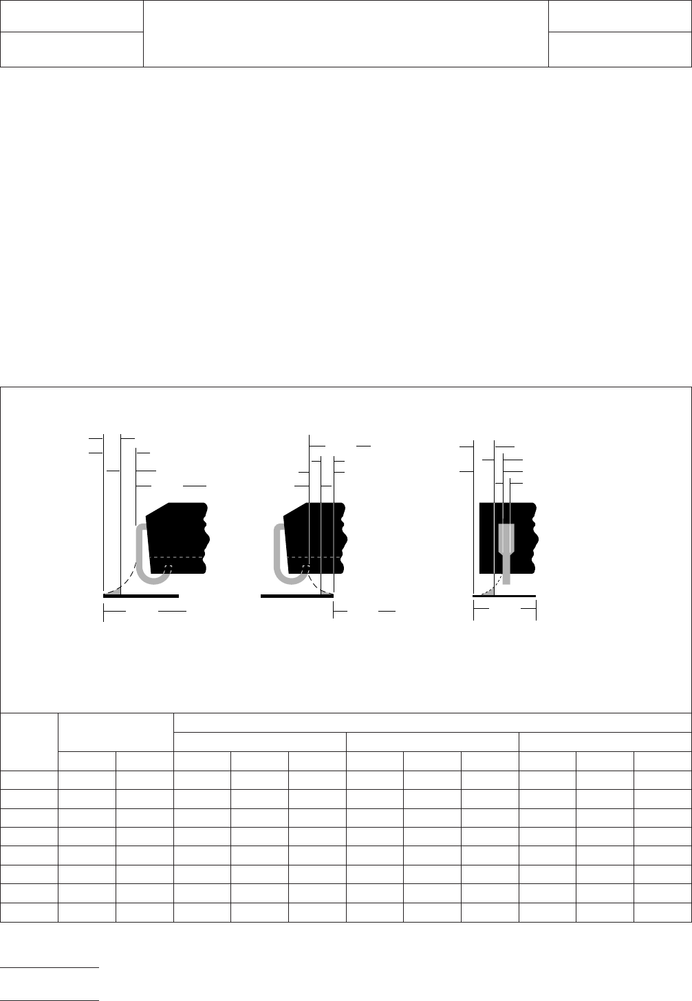
6.0 TOLERANCE AND SOLDER JOINT ANALYSIS
Figure 4 provides an analysis of tolerance assumptions and
resultant solder joints based on the land pattern dimensions
shown in Figure 3. Tolerances for the component dimensions,
the land pattern dimensions (fabrication tolerances on the
interconnecting substrate), and the component placement
equipment accuracy are all taken into consideration.
Figure 4 provides the solder joint minimums for toe, heel, and
side fillets, as discussed in Section 3.3. The tolerances are
addressed in a statistical mode, and assume even distribution
of the tolerances for component, fabrication, and placement
accuracy.
Individual tolerances for fabrication (‘‘F’’) and component
placement equipment accuracy (‘‘P’’) are assumed to be
asgiven in the table. These numbers may be modified based
on user equipment capability or fabrication criteria. Compo-
nent tolerance ranges (C
L
,C
S
, and C
W
) are derived by sub-
tracting minimum from maximum dimensions given in Figure
2. The user may also modify these numbers, based on expe-
rience with their suppliers. Modification of tolerances may
result in alternate land patterns (patterns with dimensions
other than the IPC registered land pattern dimensions).
The dimensions for minimum solder fillets at the toe, heel, or
side (J
T
,J
H
,J
S
) have been determined based on industry
empirical knowledge and reliability testing. Solder joint
strength is greatly determined by solder volume. An observ-
able solder fillet is necessary for evidence of proper wetting.
Thus, the values in the table usually provide for a positive sol-
der fillet. Nevertheless, the user may increase or decrease the
minimum value based on process capability.
RLP No.
Tolerance
Assumptions (mm)
Solder Joint
Heel (mm) Toe (mm) Side (mm)
FPC
L
J
H
min J
H
max C
S
J
T
min J
T
max C
W
J
S
min J
S
max
790A 0.10 0.10 0.25 0.37 0.51 0.75 -0.32 0.06 0.20 0.01 0.14
791A 0.10 0.10 0.25 0.40 0.54 0.75 -0.35 0.04 0.20 0.01 0.14
792A 0.10 0.10 0.25 0.36 0.50 0.75 -0.31 0.07 0.20 0.01 0.14
793A 0.10 0.10 0.25 0.39 0.53 0.75 -0.34 0.04 0.20 0.01 0.14
794A 0.10 0.10 0.25 0.35 0.49 0.75 -0.30 0.08 0.20 0.01 0.14
795A 0.10 0.10 0.25 0.41 0.55 0.75 -0.36 0.03 0.20 0.01 0.14
796A 0.10 0.10 0.25 0.37 0.51 0.75 -0.32 0.06 0.20 0.01 0.14
797A 0.10 0.10 0.25 0.36 0.50 0.75 -0.31 0.07 0.20 0.01 0.14
Figure 4 Tolerance and solder joint analysis
Zmax = Lmin + 2J
T
min + T
T
Where:
J
T
min = Minimum toe fillet
T
T
= Combined tolerances
at toe fillet
Gmin = Smax - 2J
H
min - T
H
Where:
J
H
min = Minimum heel fillet
T
H
= Combined tolerances
at heel fillet
Xmax
Xmax = Wmin + 2J
S
min + T
S
Where:
J
S
min = Minimum side fillet
T
S
= Combined tolerances
at side fillet
▼
▼
Toe Fillet
1
/2 T
S
Heel Fillet Side Fillet
J
S
max
▼
▼
▼
▼
▼
▼
▼
J
S
min
Lmin
▼
▼
Zmax
▼
▼
1
/2 T
T
J
T
min
Smax
J
H
min
1
/2 T
H
▼
▼
▼
▼
▼
▼
▼
▼
J
T
max
J
H
max
▼
▼
▼
▼
▼
▼
▼
▼
▼
▼
▼
Gmin
▼
Wmin
▼
IPC-782-12-1-4
IPC-SM-782
Subject
PLCC (Square)
Date
5/96
Section
12.1
Revision
A
Page4of4
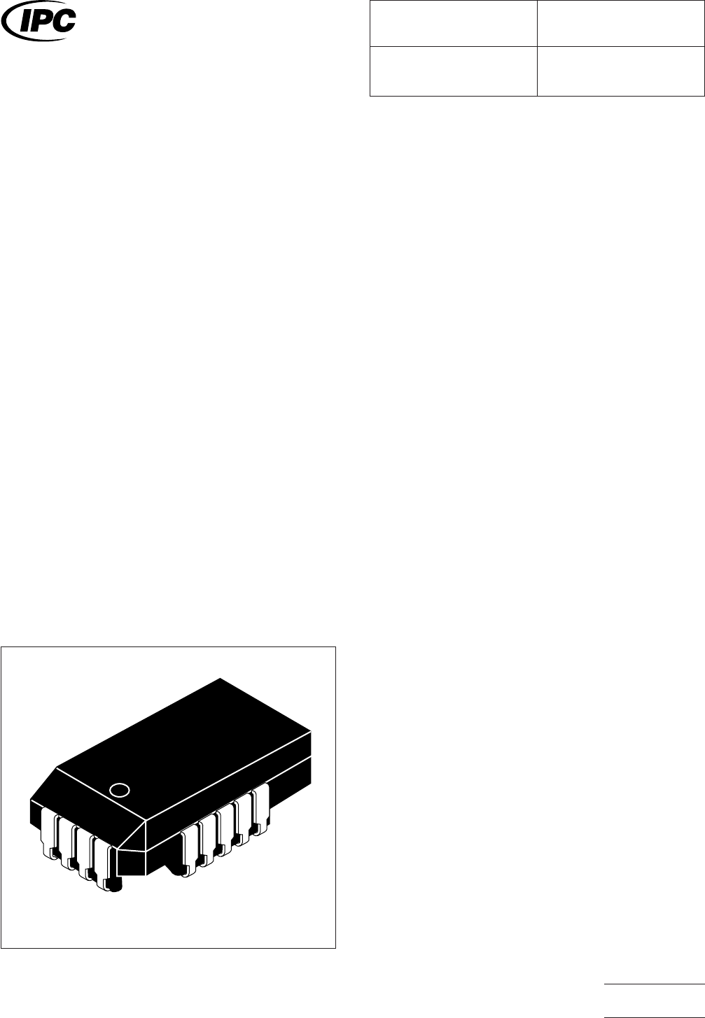
1.0 SCOPE
This subsection provides the component and land pattern
dimensions for plastic leaded chip carriers, rectangular (PLCC
components) with J leads on four sides. Basic construction of
the PLCC device is also covered. At the end of this subsec-
tion is a listing of the tolerances and target solder joint dimen-
sions used to arrive at the land pattern dimensions.
2.0 APPLICABLE DOCUMENTS
See Section 12.0 for documents applicable
to the subsections.
2.1 Electronic Industries Association (EIA)
JEDEC Publication 95
Registered and Standard Outlines for
Solid State and Related Products, ‘‘Plastic Chip Carrier
(PLCC) Family, 1.27 mm [0.050 in] Lead Spacing, Square,’’
Outline MO-052, issue ‘‘B,’’ dated 8/85
Application for copies should be addressed to:
Global Engineering Documents
1990 M Street N.W.
Washington, DC
3.0 COMPONENT DESCRIPTIONS
Plastic leaded chip carriers are employed where a hermetic
seal is not required. Other constraints include limited tempera-
ture range (typically 0°C or 70°C) and nominal environmental
protection. As with plastic DIPs, they have the advantage of
low cost as compared to ceramic packages.
3.1.1 Pre-molded Plastic Chip Carriers The pre-molded
plastic chip carrier was designed to be connected to the P&I
substrate by means of a socket. Spring pressure on both
sides of the package is intended to constrain movement as
well as allow for substrate warpage as high as 0.5%. Solder
attach to the P&I substrate is also possible. The design is also
intended to mae use of silicone encapsulant technology for
chip coverage and protection.
3.1.2 Post-molded Plastic Chip Carriers The post-
molded plastic leaded chip carrier is composed of a compos-
ite metal/dielectric assembly that includes a conductor lead
frame and a molded insulating body. Compared to the pre-
molded package which has an aperture for mounting micro-
electronic components, the post-molded package comes
complete with no apertures. In both types of plastic chip car-
riers, all necessary plating operations are performed by the
package manufacturer to eliminate tinning or plating by the
user.
The Joint Device Engineering Council (JEDEC) defines the
Type A Leaded Chip Carrier as a plastic package with leads
wrapped down and around the body on all four sides. This
package can be either directly mounted to a printed wiring
board or used with a socket. It is available with 28, 44, 52, 68,
84, 100, or 124 leads. This family is based on 1.27 mm [0.050
in] lead pitch. The original mechanical outline drawing of this
package was defined based on a premolded package. How-
ever, actual construction is not specified and the package
could be of post-molded construction.
Post-molded packages which have J-lead configuration and
are
JEDC standard MO-052, are available in 20-, 28-, 44-, 52-,
68-, 84-, 100- and 124-lead counts with the
same spacing.
3.1.3 Marking All parts shall be marked with a part number
and ‘‘Pin 1’’ location. ‘‘Pin 1’’ location may be molded into the
plastic body.
3.1.4 Carrier Package Format Bulk rods, 24 mm tape/
8–12 mm pitch is preferred for best handling. Tube carriers
are also used.
3.1.5 Resistance to Soldering Parts should be capable of
withstanding ten cycles through a standard reflow system
operating at 215°C. Each cycle shall consist of 60 seconds
exposure at 215°C. Parts must also be capable of withstand-
ing a minimum of 10 seconds immersion in molten solder at
260°C.
IPC-782-12-2-1
Figure 1 PLCC (Rectangular) construction
IPC-SM-782
Surface Mount Design
and Land Pattern Standard
Date
5/96
Section
12.2
Revision
A
Subject
PLCC (Rectangular)
Page1of4
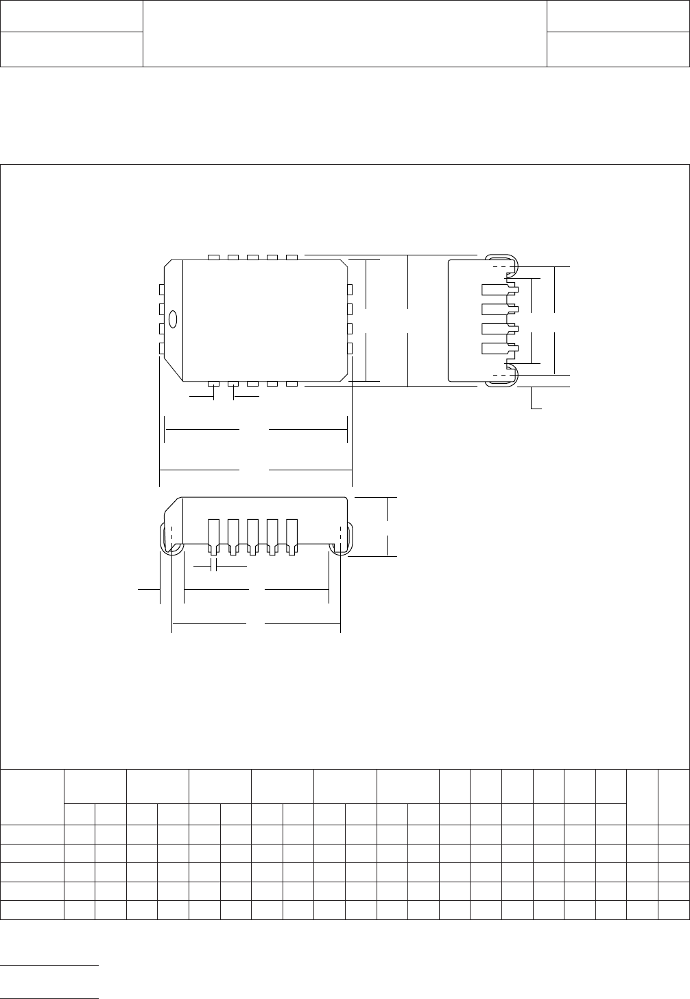
4.0 COMPONENT DIMENSIONS
Figure 2 provides the component dimensions for PLCC (Rectangular) components.
Component
Identifier
L1 (mm) S1 (mm) L2 (mm) S2 (mm) W (mm) T (mm)
A
(mm)
B
(mm)
J1
(mm)
J2
(mm)
H
(mm)
P
(mm)
Pin
Count,
Short
Side
Pin
Count,
Long
Sidemin max min max min max min max m in max min max max max ref ref max basic
PLCC/R-18 8.05 8.30 4.05 4.80 11.61 11.86 7.61 8.36 0.33 0.53 1.50 2.00 7.32 10.87 6.20 9.75 3.57 1.27 4 5
PLCC/R- 18L 8.13 8.51 4.13 4.93 13.21 13.59 9.21 10.01 0.33 0.53 1.50 2.00 7.44 12.52 6.20 11.25 3.57 1.27 4 5
PLCC/R- 22 8.13 8.51 4.13 4.93 13.21 13.59 9.21 10.01 0.33 0.53 1.50 2.00 7.44 12.52 6.20 11.25 3.57 1.27 4 7
PLCC/R-28 9.78 10.03 5.78 6.53 14.86 15.11 10.86 11.61 0.33 0.53 1.50 2.00 8.97 14.05 7.90 12.95 3.57 1.27 5 9
PLCC/R- 32 12.32 12.57 8.32 9.07 14.86 15.11 10.86 11.61 0.33 0.53 1.50 2.00 11.51 14.05 10.40 12.95 3.57 1.27 7 9
Figure 2 PLCC (Rectangular) component dimensions
1
16
▼
▼
▼
▼
▼
▼
▼
▼
▼
▼
▼
▼
▼
▼
AL
1
T
J
1
P
B
L
2
▼
▼
H
▼
▼
W
J
2
▼
▼
▼
▼
▼
S
S
1
▼
T
IPC-782-12-2-2
IPC-SM-782
Subject
PLCC (Rectangular)
Date
5/96
Section
12.2
Revision
A
Page2of4