IPC-SM-782A-表面贴装焊盘图形设计标准.pdf.pdf - 第47页
IPC-782-4-2 Figure 4–2 General description of process validation contact pattern and interconnect 5 5 5 5 5 5 5 5 + 4102 3 - + 1 2 - 4 0 3 + 4102 3 - + 1 2 - 4 0 3 + 4102 3 - + 1 2 - 4 0 3 + 4102 3 - + 1 2 - 4 0 3 + 140 …

Circuits that are shown in Figures 4–2 and 4–3 contain the
various components listed:
Test Vehicle
Primary (Top) Side
__ SITE #1
(2) 44 I/O PLCC-J
__ SITE #2
(2) 16 I/O DIP-I
__ SITE #3
(8) RC1206
(8) SOT-23
__ SITE #4
(1) 68 I/O CLCC-J
__ SITE #5
(68) I/O PLCC-J
__ SITE #6
(8) MELF 1/4W
(8) CC1825
__ SITE #8
(2) 24 I/O SOIC-L
Secondary (Bottom) Side
__ SITE #1
Empty
__ SITE #2
Empty
__ SITE #3
(8) RC1206
(8) SOT-23
__ SITE #4
Empty
__ SITE #5
Empty
__ SITE #6
(8) MELF 1/4W
(8) CC1825
__ SITE #8
Empty
Another test specimen is used for the testing of printed
board structures that are intended to provide P&I structures
used primarily for the mounting of leadless chip carriers.
This test board is described in surface mount land pattern
round robin artwork (IPC-A-48). The board is a 12-layer
multilayer board which contains 38 positions for mounting
leadless chip carriers used by an Air Force Mantech Pro-
gram to evaluate printed board and substrate materials. The
test boards produced from this artwork may contain metal
cores, or other planes that control the coefficient of thermal
expansion of the P&I structure.
The following are some examples of the type of materials
that may be used as the constraining core.
• Nonorganic materials (alumina)
• Porcelainized clad Invar materials
• Printed boards bonded to low-expansion support
(metal or nonmetal)
• Compliant layer constructions
• Metal core boards
4.2 Test Patterns—In-Process Validator Test patterns
to validate in-process conditions are encourage to be incor-
porated into the panel of a printed board assembly. These
designed-in land patterns provide special features for auto-
matic optical inspection and visual inspection.
The land patterns shown in section 8–13 are designed to
provide a clear view of the soldering characteristic such
that land geometry is visible, and solder joint evaluation
can be achieved. The same in-process validator are used to
check the registration of solder paste prior to reflow solder-
ing.
Figures 4–4 through 4–11 are illustrations from J-STD-001
that provide the key variables for meeting soldering
requirements that are necessary for various surface mount
parts. Land pattern samples provided around the periphery
of a panel, should be designed to provide clear visibility of
the solder joints shown in these figures.
4.3 Stress Testing Stress testing usually consists of tem-
perature cycling of the printed board assembly that has
been surface mounted through various extremes. The tem-
perature cycling of the assembly or a coupon may be a
standard MIL- STD-202 test method which cycles the
board from –65°C to 125°C.
Alternate temperature cycles are also available. A tempera-
ture cycle test of 400 consecutive cycles to 1000 cycles has
been identified for some assemblies. In these examples, the
ramp time from high to low temperature is 30 minutes, and
the time at the extreme is also 30 minutes. Figure 4–12
shows an example of the excursion rate of the various con-
ditions of temperature cycling.
During the cycling processes, daisy chained plated-through
holes and daisy chained solder joints, are measured during
the initial phase as to their resistance, and then monitored
for increased resistance during the thermal cycling.
Increased resistance of 30 microohms in most instances
constitutes a failure of the either the plated-through hole, or
the solder joint.
IPC-SM-782A December 1999
38
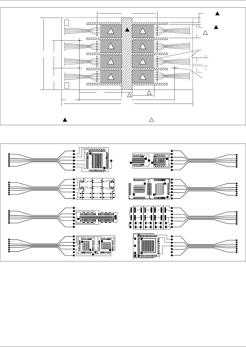
IPC-782-4-2
Figure 4–2 General description of process validation contact pattern and interconnect
5
5
5
5
5
5
5
5
+ 41023 -
+ 1 2 -
4 0 3
+ 41023 -
+ 1 2 -
4 0 3
+ 41023 -
+ 1 2 -
4 0 3
+ 41023 -
+ 1 2 -
4 0 3
+ 14032 -
+ 4 3 -
1 0 2
+ 14032 -
+ 4 3 -
1 0 2
+ 14032 -
+ 4 3 -
1 0 2
+ 14032 -
+ 4 3 -
1 0 2
5.600
▼
▼
▼
▼
I.D.I.D.
2.500
▼
▼
2.125
6.745
▼
▼
1.000
4.010
REF
▼
▼
1.490
▼
▼
4
REF
9.020
▼
▼
4
12 ± 1/32
▼
▼
Note: 1. Board G-10 thickness .040 - .036 2. Primary (top) side
3. Secondary (bottom) side, left-right mirror image
No pattern or components in those
indicated areas allowed 8 sites for test components
5
.505 REF
▼
▼
▼
▼
▼
▼
▼
▼
▼
▼
▼
.140 TYP
1.260
TYP REF
4
5
4
.035 ± .003 DIA,
96 HOLES, PTH
.600 ± .003 TYP
.100 ± .003 TYP
.125 DIA,
3 HOLES
12
3
4
56 7
8
4
2.000 REF
5
▼
▼
▼
▼
▼
All dimensions are in inches
IPC-782-4-3
Figure 4–3 Photo image of IPC-A-49 test board for primary side
December 1999 IPC-SM-782A
39
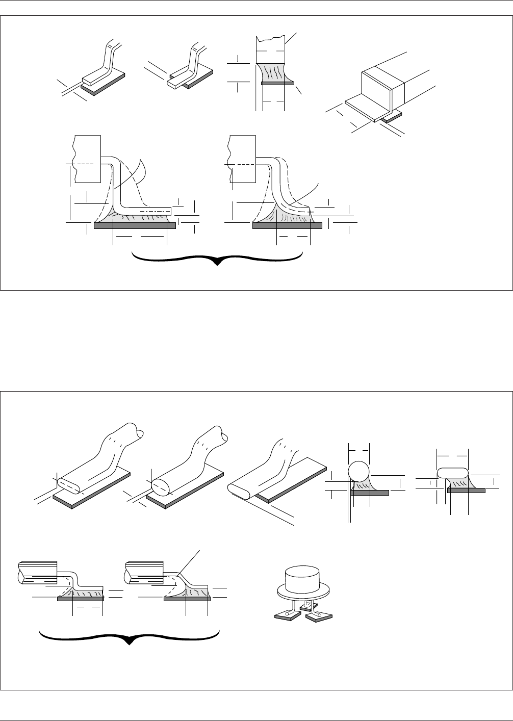
IPC-782-4-4
Figure 4–4 Flat ribbon, ‘‘L,’’ and gullwing lead joint description
B
▼
▼
A
▼
Side Overhang Toe Overhang
End Joint Width
T
▼
▼
D
▼
▼
▼
E
G
Center Line of "T"
D
▼
▼
E
▼
W = Lead Width
T = Lead Thickness
W
▼
B
▼
▼
Other Lead Configurations
▼
Side Joint Length
▼
▼
▼
▼
Lead
Land
▼
▼
▼
▼
F
▼
▼
▼
▼
CA
▼
G
▼
▼
W
T
▼
▼
▼
G
▼
F
▼
▼
▼
▼
See Note 1
Table 9–2
▼
▼
IPC-782-4-5
Figure 4–5 Round or flattened (coined) lead joint description
E
D
▼
▼
▼
▼
W = Flattened Lead
Width or Diameter
of Round Lead
T = Thickness of Lead
at Joint Site (over
land)
Side
Overhang
A
C
A
Q
G
G
C
A
B
W
▼
▼
▼
▼
Q
▼
▼
▼
▼
▼
▼
▼
▼
▼
▼
▼
Other Land
Configurations
D
▼
▼
▼
▼
▼
G
Toe
Overhang
▼
▼
A
Side Joint Length
▼
▼
▼
▼
▼
End
Joint
Width
▼
▼
W
▼
▼
▼
▼
G
E
F
▼
▼
F
▼
▼
▼
▼
See Note 1,
Table 9–3
Note: See ANSI/J-STD-001 for specific details on minimum acceptability requirements.
IPC-SM-782A December 1999
40