IPC-SM-782A-表面贴装焊盘图形设计标准.pdf.pdf - 第40页
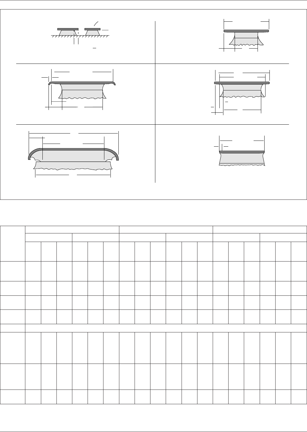
result is a scrapped PB. Since signal conductors intersect the lands from all directions, any breakout has the poten- tial to randomly disconnect conductors all over the PB. Maintaining consistent annular ring control is…
IPC-782-3-27
Figure 3–27 Conductor characteristics
▼
LaminateX
▼
Etch Factor =
V
X
An etch factor of 1/1 is usually considered practical.
Higher factors may be specified for some applications.
Resist
▼
V
▼
▼
"B" (DCW)
"E" Outgrowth
▼
▼
▼
▼
▼
▼
▼
"C" Undercut
▼
"A"
(MCW)*
Overhang
Panel Plating (Liquid Resist)
▼
▼
(OCW)*
▼
▼
"D"
"B" (DCW)*
"E" Outgrowth
▼
▼
(MCW)*
"A"
▼
▼
Pattern Plating (Liquid Resist)
▼
"B" (DCW)
(MCW)*
"C" Undercut
& Overhang
Panel Plating (Dry Film Resist)
▼
▼
"A"
▼
▼
▼
▼
▼
"D"
▼
"A"
(MCW)*
Overhang
Pattern Plating (Dry Film Resist)
▼
▼
▼
(OCW)*
"B" (DCW)*
▼
▼
▼
▼
"E" Outgrowth
▼
▼
"C" Undercut
▼
▼
"B" (DCW)*
▼
"C" Undercut
▼
Thin Clad & Pattern Plating (Dry Film Resist)
A = MCW (Minimum Conductor Width) B = DCW (Desi
g
n Conductor Width) D = OCW (Overall Conductor Width
Table 3–8 Typical Values to Be Added or Subtracted to Nominal Production to Achieve Desired Nominal Conductor Width
Description
1/2 Oz. Copper 1 Oz. Copper 2 Oz.Copper
Panel Pattern Panel Pattern Panel Pattern
Screen
Liquid
Photo
Dry
Film
Photo Screen
Liquid
Photo
Dry
Film
Photo Screen
Liquid
Photo
Dry
Film
Photo Screen
Liquid
Photo
Dry
Film
Photo Screen
Liquid
Photo
Dry
Film
Photo Screen
Liquid
Photo
Dry
Film
Photo
Subtractive
Method
Simple Etch
+25µm
[+0.0010]
+25µm
[+0.0010]
+25µm
[+0.0010]
— — — +38µ
[+0.0015]
+38µm
[+0.0015]
+38µm
[+0.0015]
— — — +63µm
[+0.0025]
+63µm
[+0.0025]
+63µm
[+0.0025]
———
Bare Copper
[PTH]
+38µ
[+0.0015]
+38µm
[+0.0015]
+50µm
[+0.0020]
-25µ
[-0.0010]
-25µm
[-0.0010]
-25µm
[-0.0010]
+50µm
[+0.0020]
+50µm
[+0.0020]
+63µm
[+00025]
0 0 +50µm
[+0.0020]
+76µm
[+0.0030]
+76µm
[+0.0030]
+89µm
[+0.0035]
+38µm
[+0.0015]
+38µm
[+0.0015]
+89µm
[+0.0035]
Tin-Lead
[PTH]
+38µm
[+0.0015]
+38µm
[+0.0015]
+50µm
[+0.0020]
-25µm
[-0.0010]
-25µm
[-0.0010]
+25µm
[+0.0010]
+50µm
[+0.0020]
+50µm
[+0.0020]
+63µm
[+0.0025]
0 0 +50µm
[+0.0020]
+76µm
[+0.0030]
+76µm
[+0.0030]
+89µm
[+0.0035]
+38µm
[+0.0015]
+38µm
[+0.0015]
+89µm
[+0.0035]
Gold Nickel
[PTH]
+38µm
[+0.0015]
+38µm
[+0.0015]
+50µm
]+0.0020]
-25µm
[-0.0010]
-25µm
[-0.0010]
+25µm
[+0.0010]
+50µm
[+0.0020]
+50µm
[+0.0020]
+63µm
[+0.0025]
0 0 +50µm
[+0.0020]
+76µm
[+0.0030]
+76µm
[+0.0030]
+89µm
[+0.0035]
+38µm
[+0.0015]
+38µm
[+0.0015]
+89µm
[+0.0015]
For Deposited Copper Thickness Equivalents
Additive
Method
Electroless
Copper
No-Etch
— — — -50µ
[-0.0020]
-25µm
[-0.0010]
-0µm
[0.0000]
— — — -76µm
[-0.0030]
-50µ
[-0.0020]
-0µ
[-0.0000]
— — — -101µ
[-0.0040]
-76µm
[-0.0030]
-0µm
[-0.0000]
Semi Additive
Method
Copper-No
Overplate
— — — -50µm
[-0.0020]
-25µm
[-0.0010]
-0µm
[-0.0000]
— — — -76µm
[-0.0030]
-50µm
[-0.0020]
-0µm
[-0.0000]
— — — -101µm
[-0.0040]
-76µm
[-0.0030]
-0µm
[-0.0000]
Tin Lead
Overplate
— — — -76µm
[-0.0030]
-50µm
[-0.0020]
-25µm
[-0.0010]
— — — -101µ
[-0.0040]
-76µm
[-0.0030]
-25µm
[-0.0010]
— — — -127µm
[-0.0050]
-101µm
[-0.0040]
-25µm
[-0.0010]
December 1999 IPC-SM-782A
31
result is a scrapped PB. Since signal conductors intersect
the lands from all directions, any breakout has the poten-
tial to randomly disconnect conductors all over the PB.
Maintaining consistent annular ring control is difficult at
best, another method had to be developed to insure connec-
tivity between lands and conductors. This method is called
filleting, corner entry or keyholing. Explained simply, each
method is intended to provide excess original copper mate-
rial at the junction where the conductor enters the land. The
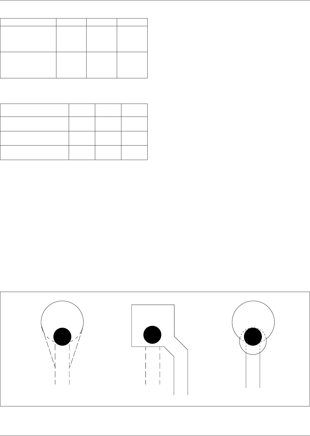
land which is filleted resembles a teardrop; it is square for
the corner entry, and looks like a figure eight for keyhol-
ing. All features point in the direction of the conductor to
permit additional misregistration allowances (see Figure
3–28).
3.6.4.5 Fabrication Panel Format Components can be
mounted on individual boards or on boards that are still
organized in panel form. Boards or panels that will be
moved by automatic handling equipment or pass through
automated operations, (parts placement, soldering, clean-
ing, etc.) must have the sides kept free of parts or active
circuitry. Special tooling and fixturing holes are generally
located within the edge clearance areas. The clearance
areas are needed to avoid interference with board handling
fixtures, guidance rails and alignment tools.
Typically a clear area of 3.0 to 5.0 mm [0.118 to 0.200 in]
must be allowed along the sides for the clearance. The
required clearance width is dependent upon the design of
the board handling and fixturing equipment. These dimen-
sions should be obtained from the equipment manufacturer
before board or panel design. (See Figure 3–29.)
For accurate fixturing, a minimum of two (and preferably
four) nonplated holes are located in the corners of the
board to provide accurate mechanical registration on board
transfer equipment. Board handling holes (typically 3.2
mm [0.125] diameter) may also be located in the clearance
areas. These holes are used by automated board handling
equipment to move boards (or panels) from station to sta-
tion in automated assembly lines. Specific sizes should be
obtained from the equipment manufacturer. In addition,
optical fiducial marks may be located near the fixturing
holes if optical alignment is used, to improve registration
(see Figure 3–14).
3.6.4.6 Board Size and Panel Construction In order to
fully utilize the automation technology associated with sur-
face mount components, a designer should consider how a
printed board or P&I structure will be fabricated,
assembled and tested. Each of these processes, because of
the particular equipment used, requires fixturing which will
Table 3–9 Conductor Width Tolerances
Feature Level A Level B Level C
Without plating +0.05
–0.10
[+0.002]
[–0.004]
+0.03
–0.05
[+0.001]
[–0.002]
+0.02
–0.04
[+0.0008]
[–0.0016]
With plating +0.10
–0.10
[+0.004]
[–0.004]
+0.08
–0.08
[+0.003]
[–0.003]
+0.05
–0.05
[+0.002]
[–0.002]
Table 3–10 Conductive Pattern Location Tolerances
Greatest Board/
X, Y Dimension Level A Level B Level C
Up to 300 mm [12.0] 0.30 mm
[0.012]
0.20 mm
[0.008]
0.10 mm
[0.004]
Up to 450 mm [18.0] 0.40 mm
[0.016]
0.30 mm
[0.012]
0.20 mm
[0.008]
Up to 600 mm [24.0] 0.40 mm
[0.016]
0.30 mm
[0.012]
0.20 mm
[0.008]
IPC-782-3-28
Figure 3–28 Examples of modified landscapes
Corner EntryFilleting
Key
Holing
IPC-SM-782A December 1999
32
affect or dictate certain facets of the board layout. Tooling
holes, panel size, component orientation and clearance
areas (both component and conductor) on the primary and
secondary sides of the board are all equipment and process
dependent.
To produce a cost effective layout through optimum base
material utilization a designer should consult with the
board fabricator to determine optimum panel size. The
board should be designed to utilize the manufacturer’s sug-
gested usable area. Smaller boards can be ganged or nested
on this same panel size to simplify fixturing and reduce
excessive handling during assembly. Most manufacturers
will suggest various methods of retaining assemblies in
panels. A method should be chosen taking the assembly
and test processes into consideration.
Figure 3–29 shows the typical use of a copper clad glass
laminate panel. See IPC-D-322 for panel to board relation-
ship.
Small boards can effectively be arranged on a single work-
ing panel, if the designer works closely with manufactur-
ing. These are commonly called nested panels or pallets.
Panel construction may include several boards arranged in
a matrix or simply one board requiring additional material
retained for efficient assembly processing. The large board
or several smaller boards are retained in the panels and
separated after all assembly processes are completed.
Excising or separating the individual boards from the panel
must be planned as well. Several methods are used to retain
circuits in a panel, including V-groove scoring and routed
slot with break-away tabs.
V-groove scoring is generally provided on both surfaces of
the board, and only in a straight line. A small cross section
of board material is retained at the break line. An allow-
ance for the scoring angle must be made as well. Conduc-
tors that are located too close to the score groove will be
IPC-782-3-29
Figure 3–29 Typical copper glass laminate panel
▼
The keepout zone defined in this illustration is typical for in-line assembly automation using reflow and wave solder processes.
▼
X
Typical Finished Panel
for Automated SMT
Assembly Equipment
Showing two
printed board assemblies
▼
300mm
[12.0]
▼
▼
3.0mm
[0.12]
▼
▼
5.0mm
[.2.0]
▼
10mm [0.40]
▼
5mm [0.20]
▼▼
▼
3.0mm
[0.12]
Keep Clear
▼
Primary Component Side
Secondary Component Side
▼
▼
12.0mm
max.
[0.500]
5mm
[2.0] min.
DIRECTION OF FLOW
KEEPOUT ZONE
KEEPOUT ZONE
▼
▼
▼
December 1999 IPC-SM-782A
33