IPC-SM-782A-表面贴装焊盘图形设计标准.pdf.pdf - 第60页
machines. This geometry results in a low-profile intercon- nection pattern with excellent high-speed electrical charac- teristics and a density normally associated with thick-film technology . 6.5 Constraining Core P&I…

Table 6–1 Packaging and Interconnecting Structure Comparison
Type Major Advantages Major Disadvantages Comments
Organic Base Substrate
Epoxy Fiberglass Substrate size, weight,
reworkable, dielectric
properties, conventional board
processing
Thermal conductivity, X, Y and
Z axis CTE
Because of its high X–Y plane
CTE, it should be limited to
environments and applications
with small changes in
temperature and/or small
packages.
Polyimide Fiberglass Same as Epoxy Fiberglass plus
high temperature X–Y axis
CTE, substrate size, weight,
reworkable, dielectric
properties, high Tg.
Thermal conductivity, Z-axis
CTE, moisture absorption
Same as Epoxy Fiberglass
Epoxy Aramid Fiber Same as Epoxy Fiberglass,
X–Y axis CTE, substrate size,
lightest weight, reworkable,
dielectric properties
Thermal conductivity, Z-axis
CTE, resin microcracking, Z
axis CTE, water absorption
Volume fraction of fiber can be
controlled to tailor X–Y CTE.
Resin selection critical to
reducing resin micro-cracks
Polyimide Aramid Fiber Same as Epoxy Aramid Fiber,
X–axis CTE, substrate size,
weight, reworkable, dielectric
properties
Thermal conductivity, Z–axis
CTE, resin microcracking,
water absorption
Same as Epoxy Aramid Fiber
Polyimide Quartz (Fused Silica) Same as Polyimide Aramid
Fiber, X–Y axis CTE, substrate
size, weight, reworkable,
dielectric properties
Thermal conductivity, Z axis
CTE, drilling, availability, cost,
low resin content required
Volume fraction of fiber can be
controlled to tailor X–Y CTE.
Drill wearout higher than with
fiberglass.
Fiberglass/Aramid Composite
Fiber
Same as Polyimide Aramid
Fiber, no surface microcracks,
Z axis CTE, substrate size,
weight, reworkable, dielectric
properties
Thermal conductivity, X and Y
axis CTE, water absorption,
process solution entrapment
Resin microcracks are confined
to internal layers and cannot
damage external circuitry.
Fiberglass/Teflon® Laminates Dielectric constant, high
temperature
Same as Epoxy Fiberglass, low
temperature stability, thermal
conductivity, X and Y axis CTE
Suitable for high speed logic
applications.
Same as Epoxy Fiberglass.
Flexible Dielectric Light weight, minimal concern
to CTE, configuration flexibility
Size, cost, Z-axis expansion Rigid-flexible boards offer
trade-off compromises.
Thermoplastic 3–D configurations, low
high-volume cost
High injection-molding setup
costs
Relatively new for these
applications
Non-Organic Base
Alumina (Ceramic) CTE, thermal conductivity,
conventional thick film or thin
film processing, integrated
resistors
Substrate size, rework
limitations, weight, cost, brittle,
dielectric constant
Most widely used for hybrid
circuit technology
Supporting Plane
Printed Board Bonded to Plane
Support (Metal or Non-Metal)
Substrate size, reworkability,
dielectric properties,
conventional board processing,
X–Y axis CTE, stiffness,
shielding, cooling
Weight The thickness/CTE of the metal
core can be varied along with
the board thickness, to tailor
the overall CTE of the
composite.
Sequential Processed Board
with Supporting Plane Core
Same as board bonded to
supporting plane
Weight Same as board bonded to
supporting plane.
Discrete Wire High-speed interconnections.
Good thermal and electrical
features.
Licensed process.
Requires special equipment.
Same as board bonded to
low-expansion metal support
plane.
Constraining Core
Porcelainized Copper Clad
Invar
Same as Alumina. Reworkability, compatible thick
film materials.
Thick film materials are still
under development.
Printed Board Bonded with
Constraining Metal Core
Same as board bonded to low
expansion metal cores,
stiffness, thermal conductivity,
low weight.
Cost, microcracking. The thickness of the graphite
and board can be varied to
tailor the overall CTE of the
composite.
Compliant Layer Structures Substrate size, dielectric
properties, X–Y axis, CTE.
Z axis CTE, thermal
conductivity.
Compliant layer absorbs
difference in CTE between
ceramic package and
substrate.
December 1999 IPC-SM-782A
51
machines. This geometry results in a low-profile intercon-
nection pattern with excellent high-speed electrical charac-
teristics and a density normally associated with thick-film
technology.
6.5 Constraining Core P&I Structures As with
supporting- plane P&IS, one or more supporting metallic
or non-metallic planes can serve as a stiffener, heatsink,
and/or CTE constraint in constraining core P&IS struc-
tures.
6.5.1 Porcelainized-Metal (Metal Core) Structures An
integral core of low-expansion metal (e.g., copper-clad
Invar), can reduce the CTE of porcelainized-metal P&I
structures so that it closely matches the CTE of the ceramic
chip carrier. Also, the P&I structure size is virtually unlim-
ited. However, the low melting point of the porcelain
requires low-firing-temperature conductor, dielectric and
resistor inks.
A number of composite P&I structures use leadless compo-
nents. An integral material with a lower CTE than that of
the printed boards controls the CTE of these structures.
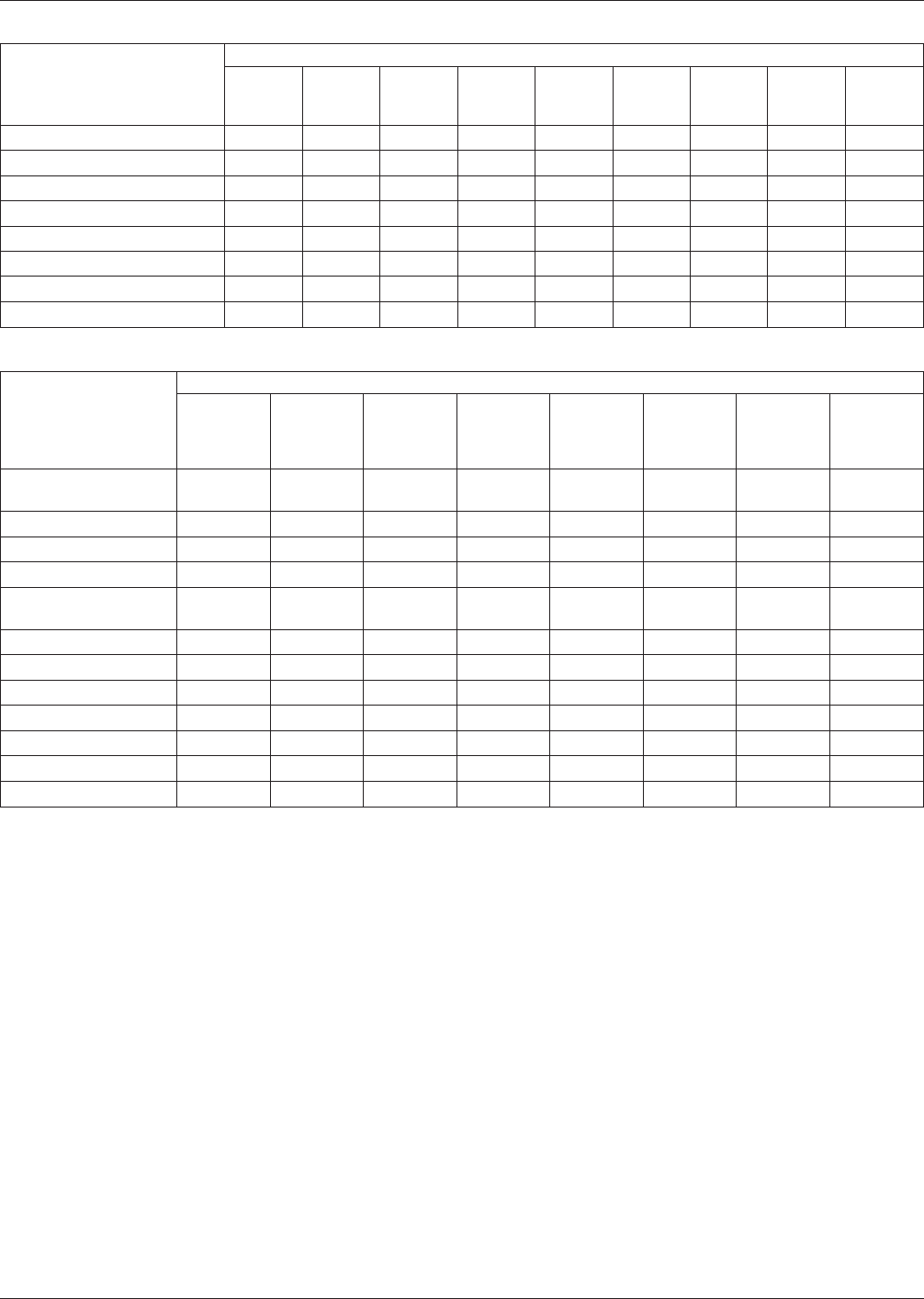
Table 6–2 P & I Structure Selection Considerations
Design Parameters
Material Properties
Transition
Temperature
Coefficient
of Thermal
Expansion
Thermal
Conductivity
Tensile
Modulus
Flexural
Modulus
Dielectric
Constant
Volume
Resistivity
Surface
Resistivity
Moisture
Absorption
Temperature & Power Cycling XXXX
Vibration X X
Mechanical Shock X X
Temperature & Humidity X X XXXX
Power Density X X
Chip Carrier Size X X
Circuit Density XXX
Circuit Speed XXX
Table 6–3 P & I Structure Material Properties
Material
Material Properties
Glass
Transition
Temperature
XY
Coefficient
of Thermal
Expansion
Thermal
Conductivity
XY Tensile
Modulus
Dielectric
Constant
Volume
Resistivity
Surface
Resistivity
Moisture
Absorption
Unit of measure (°C) (PPM/°C)
(note 4)
(W/M°C) (PSI x
10
–6
)
(At 1 MHz) (Ohms/cm) (Ohms) (Percent)
Epoxy Fiberglass 125 13–18 0.16 2.5 4.8 10
12
10
13
0.10
Polyimide Fiberglass 250 12–16 0.35 2.8 4.8 10
14
10
13
0.35
Epoxy Aramid Fiber 125 6–8 0.12 4.4 3.9 10
16
10
16
0.85
Polyimide Aramid
Fiber
250 3–7 0.15 4.0 3.6 10
12
10
12
1.50
Polyimide Quartz 250 6–8 0.30 4.0 10
9
10
8
0.50
Fiberglass/Teflon 75 20 0.26 0.2 2.3 10
10
10
11
1.10
Thermoplastic Resin 190 25–30 3–4 10
17
10
13
NA
Alumina–Beryllia NA 5–7 21.0 44.0 8.0 10
14
Aluminum (6061 T–6) NA 23.6 200 10 NA 10
6
NA
Copper (CDA101) NA 17.3 400 17 NA 10
6
Copper-Clad Invar NA 3–6 150XY/20Z 17–22 NA 10
6
NA
Notes:
1. These materials can be tailored to provide a wide variety of material properties based on resins, core materials, core thickness,
and processing methods.
2. The X and Y expansion is controlled by the core material and only the Z axis is free to expand unrestrained. Where the Tg will be
the same as the reinforced resin system used.
3. When used, a compliant layer will conform to the CTE of the base material and to the ceramic component, therefore reducing the
strain between the component and P&I structure.
4. Figures are below glass transition temperature, are dependent on method of measurement and percentage of resin content.
NA = Not Applicable
IPC-SM-782A December 1999
52

7.0 ASSEMBLY CONSIDERATIONS FOR SURFACE
MOUNT TECHNOLOGY (SMT)
The smaller size of surface mount components and the
option of mounting them on either or both sides of the
packaging and interconnecting structure reduces board real
estate significantly. The type of SMT assembly is basically
determined by the type of surface mount components to be
used; see paragraph 3.6.1.5 for a description of types and
classes.
This section will briefly discuss the assembly process
issues for SMT assemblies. For additional information, see
IPC-SM-780 and IPC-CM-770. The reader is also directed
to IPC-9191 for continued process improvement.
7.1 SMT Assembly Process Sequence The SMT assem-
blies are soldered by reflow (vapor phase, infra red, hot air,
convection, laser, conduction belt) and/or wave soldering
processes depending upon the mix of surface mount and
through hole mount components.
The process sequence for Type 2c SMT is shown in Figure
7–1. The leaded components are automatically or hand
inserted. The assembly is turned over and adhesive applied.
Then the surface mount components are placed by a pick-
and-place machine, the adhesive is cured, the assembly is
turned over again and the wave soldering process is used to
solder both leaded and surface mount components in a
single operation. Finally the assembly is cleaned,
inspected, repaired if necessary, and tested.
The process sequence for Type 1b SMT is shown in Figure
7–2. Solder paste is applied, components are placed, the
assembly is reflow soldered and cleaned. For Type 2b SMT
assemblies, the board is turned over and the process
sequence just described is repeated.
The process sequence for Type 2c Complex SMT, shown in
Figure 7–3, is simply a combination of SMT processes.
7.2 Substrate Preparation Adhesive, Solder Paste
7.2.1 Adhesive Application
In wave soldering of SMT,
selection and application of adhesive plays a critical role.
With too much adhesive, the adhesive gets on lands result-
ing in poor solder fillets. Too little adhesive will fail to
accomplish its objective of holding parts to the bottom of
the board during wave soldering.
A good adhesive has desirable properties such as being
single part, colored, long shelf life, ease of application, and
an adequate bond strength with short cure time. In addition,
after curing and soldering, the adhesive should remain
moisture resistant, nonconductive, noncorrosive, and be
reworkable. There are various companies that supply adhe-
sives for SMT. Some of these adhesives require UV cure
followed by IR; others can be cured in IR (infrared) or
conventional ovens.
For adhesive cure, temperature plays a bigger role than the
time. Only 10°C temperature variation from the recom-
mended cure temperature may cause loss of chips in the
wave (under cure) or difficult repair problems (overcure).
7.2.2 Conductive Epoxy Some applications for SMT
attachment use conductive epoxy as the attachment mate-
rial. Adequate conductive epoxy volume is essential at the
location of the epoxy on the land.
Unlike solder paste which is redistributed when reflowed,
conductive epoxies must be properly controlled to ensure
adequate joint strength. Also, component placement must
be controlled in order to prevent epoxy squeeze-out, and
possible shorts to adjacent lands.
7.2.3 Solder Application, Paste, and Preform Solder
paste plays an important role in reflow soldering. The paste
acts as an adhesive before reflow. It contains flux, solvent,
suspending agent, and alloy of the desired composition. In
selecting a particular paste, rheological characteristics such
as viscosity, dispensing, screening or stencil, flow, and
spread are very important. Susceptibility of the paste to
solder ball formation and wetting characteristics are also
important.
Solder paste is applied on the lands before component
placement either by screening, stenciling, or syringe.
Screens are made from stainless steel or polyester wire
mesh and stencils are etched stainless steel, brass sheets
and other stable alloy
Stencils are preferred for high volume applications. They
are more durable than screens, easier to align, and can be
used to apply a thicker layer of solder paste.
Solder preforms are sometimes used for through-board-
mounted devices. They come in required size and compo-
sition, with flux either inside the preforms, or as a coating
or without flux. They may be cost effective to avoid wave
solder processes if there are only a few leaded components
on the board.
7.2.4 Solid Solder Deposition
7.3 Component Placement
The accuracy requirements
almost make it mandatory to use autoplacement machines
for placing surface mount components on the board. Selec-
tion of the appropriate autoplacement machine is dictated
by the type of parts to be placed and their volume. There
are basically four types of autoplacement machines
available.
• In-line placement
• Simultaneous placement
• Sequential placement
• Sequential/simultaneous placement
December 1999 IPC-SM-782A
53