IPC-SM-782A-表面贴装焊盘图形设计标准.pdf.pdf - 第192页
contacts is typically 1.0 mm, 1.27 mm and 1.5 mm. The con- tacts accommodate the electrical and mechanical interface between device and host interconnecting structure (printed board). The contact material will allow conv…
1.0 INTRODUCTION
This section covers land pattern recommendations for ball
grid array (BGA) contact devices. Each subsection contains
information in accordance with the following format.
1.0 Scope
2.0 Applicable Documents
3.0 General Component Description
4.0 Component Outline
5.0 Land Pattern Dimensions
6.0 Land Pattern Analysis
The following is the table of contents for this section:
Table of Contents
Components with Ball Grid Array Contacts
Section
14.1
14.2
Family
PBGA
R-PBGA
2.0 APPLICABLE DOCUMENTS
The following documents, of the issue in effect on the current
revision date of this section, form a part of this specification to
the extent specified herein.
2.1 Electronic Industries Alliance (EIA) Automated Com-
ponent Handling (ACH) Convention
1
ACH:EIA-481-A Taping of Surface Mount Components for
Automated Placement.
ACH:EIA-481-3 32, 44 and 56 mm Embossed Carrier Tap-
ing of Surface Mount Components for Automated Handling.
2.2 Joint Electronic Device Engineering Council
2
JEDEC Publication 95 Registered and Standard Outlines for
Solid State and Related Products:
• Plastic Ball Grid Array (PBGA), MO-151 and MS-028
• Thick Matrix Tray for Handling/Shipping of Ball Grid Array
Packages, CO-028
• Thin Matrix Tray for Shipping and Handling of Ball Grid
Packages, CO-029.
2.3 Electronic Industries Association of Japan (EIAJ)
3
EIAJ-ED-7404 General Rules for the Preparation of Outline
Drawings of Integrated Circuits
2.4 International Electrotechnical Commission (IEC)
4
IEC-97 Requirements for Uniform Grid Elements
IEC-60191-2 Mechanical Standardization of Solid State
Products
2.5 Joint Industry Standards
5
J-STD-013 Implementation of Ball Grid Array and Other High
Density Technology
3.0 GENERAL INFORMATION
3.1 Component Description
The Grid Array device family
includes square and rectangular package configurations and
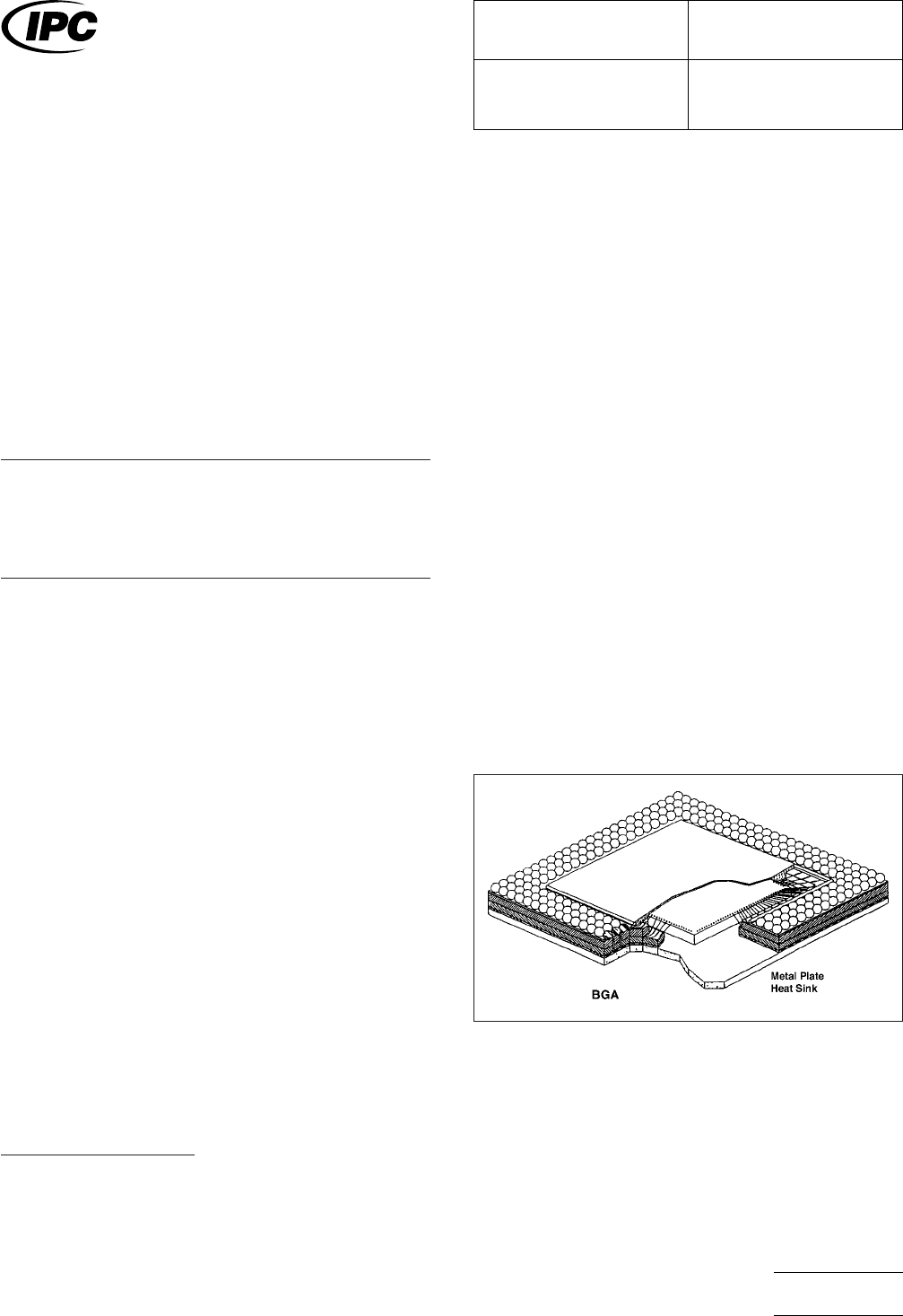
is furnished in a variety of base materials. Figure 3-1 shows
the elements of a BGA. Base material serves as a mounting
structure for attaching the die. Depending on the physical
characteristics of the material, flip-chip or wire bond technolo-
gies may be employed to route the signal from the die bond
pads to the array matrix on the base interface structure. Fig-
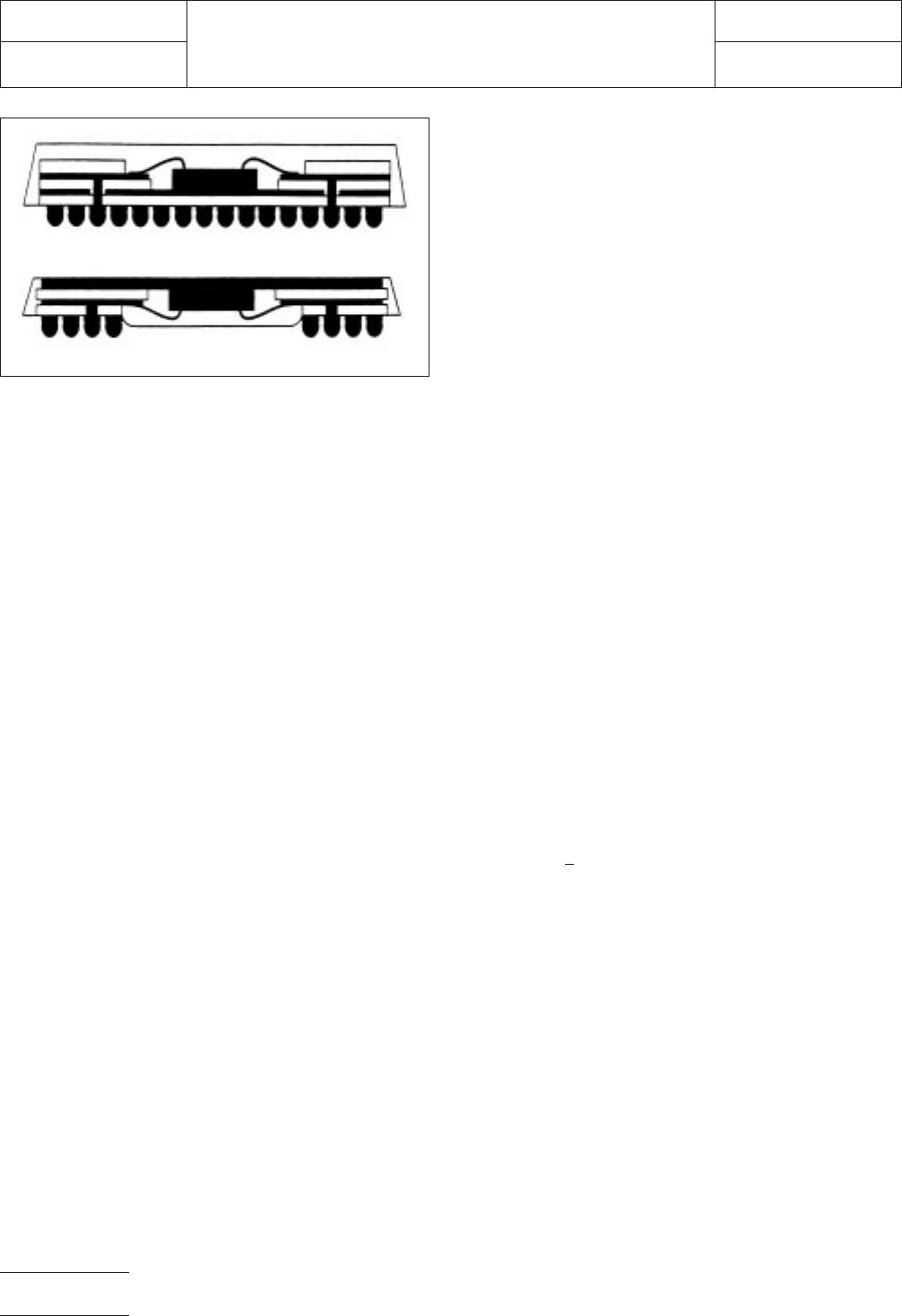
ure 3-2 compares the top surface attached die to the cavity
down configuration.
The interface contact or grid is arranged in a uniform column
and row format. The standard basic spacing or pitch for the
1. EIA: 2500 Wilson Blvd., Arlington, VA, 22201-3834, USA.
2. JEDEC: 2500 Wilson Blvd., Arlington, VA, 22201-3834, USA.
3. EIAJ: 8th Toyo Kaiji Building 6F, 1-5-13 Nishi-Shinbashi, Minato-ku Tokyo 105, Japan.
4. IEC: 3 rue de Verembe, PO Box 131-1211, Geneva 20, Switzerland.
5. IPC: 2215 Sanders Road, Northbrook, IL 60062
IPC-782143-1
Figure 3-1 Ball Grid Array IC package example
IPC-SM-782
Surface Mount Design
and Land Pattern Standard
Date
4/99
Section
14.0
Revision
—
Subject
Components with Ball
Grid Array Contacts
Page1of6
contacts is typically 1.0 mm, 1.27 mm and 1.5 mm. The con-
tacts accommodate the electrical and mechanical interface
between device and host interconnecting structure (printed
board). The contact material will allow conventional reflow sol-
der or other attachment processes.
3.2 Marking The Ball Array device families are generally
marked with the manufacturers name or symbol, part number,
date code and orientation mark in the corner near contact
location A1.
3.3 Carrier Package Format Devices may be furnished in
matrix tray or tape and reel packaging formats. Tape and reel
packaging is generally preferred for high volume assembly.
Plastic trays and reels must be transported and stored in
moisture proof containers. When plastic array devices are
exposed to the environment for an extended period of time,
moisture may absorb into the device. The absorbed moisture,
if excessive, may expand (when exposed to higher tempera-
tures typical of reflow solder process), causing cracking and
other physical damage.
3.4 Assembly Process Conditions The Grid Array
devices are typically attached to the host interface structure
using eutectic solder alloy however, optional methods of
attachment may include electrically conductive epoxy or poly-
mer. Array package assembly should not require specialized
equipment or processes beyond that used for vision assisted
SMT pick and place.
4.0 GENERAL CONFIGURATION ISSUES
4.1 Device Outlines
The Grid Array package outlines
detailed in this document are furnished in JEDEC Publication
95. The overall outline specification for the array device allows
a great deal of flexibility as far as lead pitch, contact matrix
pattern and construction. The JEDEC standards allow for die
attachment on either side of the interface structure (cavity up
or cavity down). Refer to J-STD-013 for further definition and
interconnect schemes for BGAs.
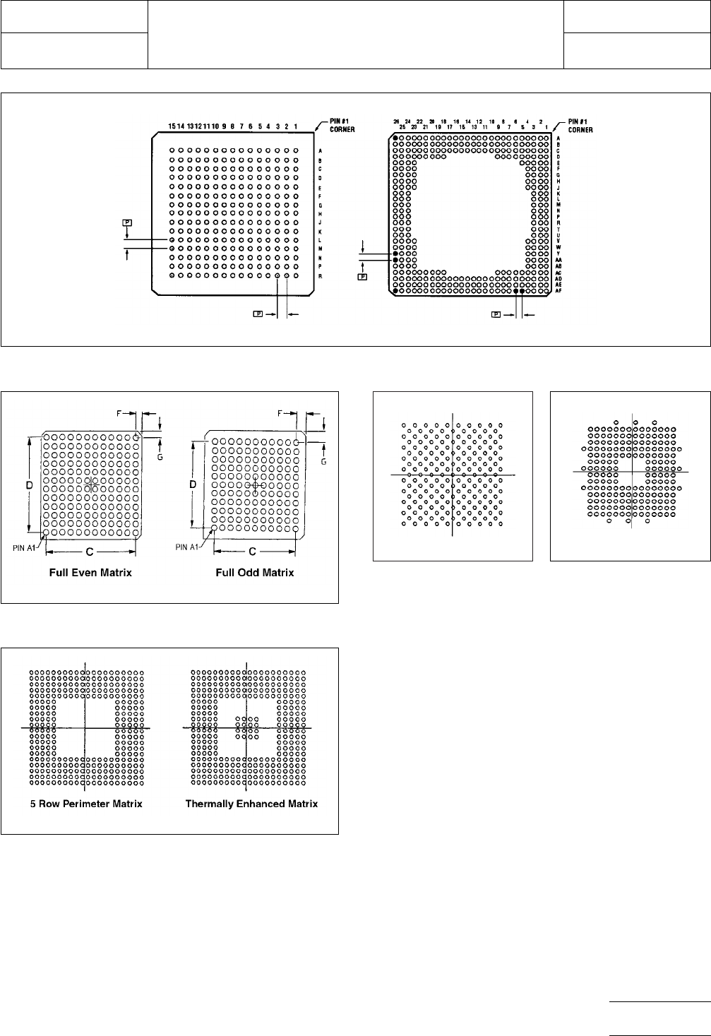
The example shown in Figure 4-1 illustrates two 225 I/O
devices with a common package outline but, with the variation
of contact pitch, a unique matrix format is provided.
4.2 Contact Matrix Options Contacts may be distributed
in a uniform pattern, however the matrix is always centered
about the centerline of the package (see Figure 4-2). Contact
depopulation is permitted at the discretion of the device
manufacturer. Contact patterns can usually be described in
the following methods: full even matrix, full odd matrix, perim-
eter matrix, or staggered matrix.
4.2.1 Full Matrix For a given package size, there are two
full matrix possibilities: even and odd. One of them is the larg-
est matrix that theoretically could fit on the package, given the
size and pitch of the contacts. The other matrix is smaller by
one row and column. See Figure 4-2.
4.2.2 Perimeter Matrix A perimeter matrix is achieved by
removing an array of contacts from the center of the matrix.
Center-depopulation does not affect the centerline of the
matrix. See Figure 4-3. In addition, Perimeter matrices are
usually described by the number of contact perimeters.
4.2.3 Thermally Enhanced Matrix A thermally enhanced
matrix is a perimeter matrix with contacts added back in the
center. See Figure 4-3.
4.2.4 Staggered Matrix A staggered matrix is defined by
the removal of every other contact in an interstitial pattern.
This provides an effective minimum center-to-center contact
spacing of
√
2 x pitch of the full matrix. See Figure 4-4. In
order to retain the A1 contact position, the staggered matrix
must be developed using a full odd matrix.
4.3 Selective Depopulation In addition to depopulation
methods which lead to the matrices described above, con-
tacts may be removed selectively. Selective depopulation can
be accomplished in any manner as long as the pattern matrix
is not shifted from the center of the package outline. See Fig-
ure 4-5.
4.4 Attachment Site Planning The attachment site or
land pattern geometry recommended for BGA devices is
round with the diameter adjusted to meet contact pitch and
size variation. The diameter of the land should be no larger
than the diameter of the land at the package interface and is
typically 20% smaller than the normal diameter specified for
the ball contact for pitches greater than 1.0 mm and 10%
IPC-782143-2
Figure 3-2 Examples of plastic BGA package
configurations
IPC-SM-782A
Subject
Components with Ball Grid Array Contacts
Date
4/99
Section
14.0
Revision
—
Page2of6
smaller for pitches less than 1.0 mm. Refer to the manufac-
turer specification before finalizing land pattern array and
geometry.
4.4.1 Copper Defined Land Pattern The land patterns
described are defined by the etched copper. Solder mask
clearance should be a minimum of 0.075 mm from the etched
copper land. For applications requiring a clearance that is less
than recommended, consult with the printed board supplier.
4.4.2 Solder Mask Defined Land Pattern If solder mask
defined patterns are used, then adjust land pattern diameter
accordingly. See Section 6.0.
4.5 Defining Contact Assignment Array contact identifi-
cation is assigned by the column and row location. For
example, A1 contact position is always at an outside corner
position with alpha characters arranged in a vertical (row) pat-
tern from top to bottom. Numeric characters are assigned in
a horizontal (column) axis (I, O, Q, S, X and Z are omitted). See
Figure 4-6.
The designer should note that the A1 position is at the upper
left hand corner when the device is viewed from the top. Con-
tact pattern is defined when viewed from the bottom. The land
pattern provided on the host substrate is opposite of the con-
tact pattern (with A1 contact position again at the upper left).
IPC-782144-4
Figure 4-4 Staggered
matrix
IPC-782144-5
Figure 4-5 Selective
depopulation
IPC-782144-1
Figure 4-1 Bottom view of BGA devices
IPC-782144-2
Figure 4-2 One package size, two full matrices
IPC-782144-3
Figure 4-3 Perimeter and thermally enhanced matrices
IPC-SM-782A
Subject
Components with Ball Grid Array Contacts
Date
4/99
Section
14.0
Revision
—
Page3of6