IPC-SM-782A-表面贴装焊盘图形设计标准.pdf.pdf - 第44页
3.7.2 Soldermask Issues Rework of Surface Mount Assemblies due to soldermask related defects is cited as a major cause of problems by assembly people. Following are two classes of assembly problems caused by improp- erly…
boards may favor the lands only (pad cap) concept. The
pad cap concept has two yield improvement benefits: 1) no
fine conductor geometries on the outer layers because they
are buried in the inner layers where conductor width con-
trol is significantly easier, and 2) the need for soldermask
is reduced or eliminated because there are no small spaces
to protect from the soldering process.
In general, an 8-layer printed board, with lands only on the
outer layer, is similar in cost to a 6-layer printed board with
solder mask, assuming both have SMT geometries. The
primary reason for this is that some PB fabricators are
realizing about a 12% yield improvement by not having the
fine line conductors on the outer layers.
The benefits of pad caps continue into the assembly pro-
cess by increasing yields through the reduction of solder
shorts or bridging. The pad cap concept provides 100%
testability, thus testing benefits are both economical and
practical.
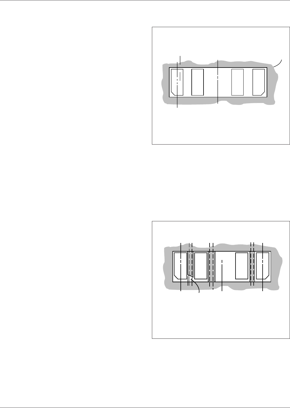
IPC-782-3-31
Figure 3–31 Breakaway (routed pattern)
[75mm 3.0] TYP
Approximately
Center to Center Spacing
▼
▼
▼
▼ ▼
▼
▼
▼
▼
0.4mm
[0.159]
Tooling Hole
5.0mm
[0.197]
10mm [0.40]
Depending on PWB
Outline Design
5.0mm
[0.197]
12.5mm
[0.50]
Breakaways
▼
▼
▼
▼
▼
1.25mm [0.050] TYP
0.8mm [0.031]
Dia Thru XX PL
▼
▼
▼
▼
2.25mm
[0.90]
1.2mm [0.047]
R TYP
4.5mm
[0.180]
REF
Detail of Breakaway
▼
▼
0.4mm
[.016]
LOW STRESS (MOUSE BITE) BREAKAWAY
IPC-782-3-32
Figure 3–32 Routed slots
Break Line
▼
December 1999 IPC-SM-782A
35
3.7.2 Soldermask Issues Rework of Surface Mount
Assemblies due to soldermask related defects is cited as a
major cause of problems by assembly people. Following
are two classes of assembly problems caused by improp-
erly applied soldermask: 1) soldermask on the component
mounting lands; 2) insufficient soldermask coverage of
unrelated circuit features in close proximity to the compo-
nent mounting land.
Regarding soldermask on the lands and assuming that the
solderability requirements of the component leads and
board mounting lands have been met, the solder paste com-
position, viscosity, and aging are within limits, and the
thermal profile of the reflow oven is correct, the only other
variable which could be detrimental to good solder joint
integrity is soldermask material on the lands. If there is any
soldermask (even if invisible to the naked eye) on the lands
during reflow, solder joint integrity can be lost through
improper surface wetting.
The second class of assembly defects is created when there
is insufficient soldermask coverage of circuitry in close
proximity to the component mounting land leading to sol-
der shorts or bridging. The majority of SMT designs incor-
porate very small geometries of 0.15–0.2 mm [0.006–
0.008 in] conductors and spacing on the outer layers of the
printed board. Designing a soldermask to cover a 0.15 mm
[0.006 in] conductor and only half of the 0.15 mm [0.006
in] space between the conductor and the land is easy
enough to accomplish during design. However, photo
imaged soldermask will overcome most of the above issues
(see Section 3.7.4).
Close examination of solder bridging on Printed Board
Assemblies will reveal that most of the bridging actually
occurs between the component leads above the surface of
the PB, and not between the lands on the board. Even if a
soldermask has sufficient resolution and registration to pro-
vide a solder dam between lands, it still may not prevent
bridging between the leads. Soldermask should not, and
can not, be expected to compensate for deficiencies in the
soldering process if the assembly uses Fine Pitch compo-
nents.
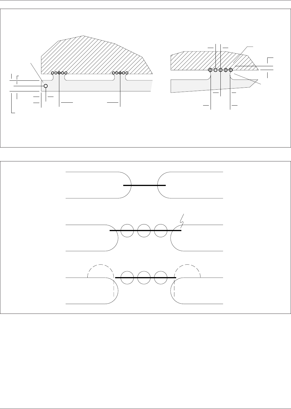
3.7.3 Solder Mask Clearances A soldermask may be
used to isolate the land pattern from other conductive fea-
tures on the board such as vias, lands or conductors. Where
no conductors run between lands, a simple gang mask can
be used as shown in Figure 3–33. Tolerance requirements
for this design can generally be met by a screen printed
soldermask. A 0.38 mm [0.015 in] spacing could be accept-
able. Any class of solder mask per IPC-SM-840 could be
applied. The most commonly chosen solder mask would be
a Class 3 mask because of its higher temperature character-
istics. Due to the close proximity of the solder mask to the
land pattern, care must be taken in choosing a mask that
has low flow and low solvent-bleed characteristics to avoid
land pattern contamination.
For land pattern designs with routed conductors between
lands (Figure 3–34) the tolerance requirement would
require a photo-imageable soldermask. This is necessary
because of the tight tolerance needed to cover the conduc-
tors without encroaching on the land area. A 0.08 to 0.125
mm [0.003 to 0.005 in] clearance is required with this type
of design.
3.7.4 Soldermask Types Solder mask coatings are avail-
able in two forms, liquid and dry film. The polymer mask
material is applied using several process methods and are
furnished in varying thicknesses. As an example, liquid
materials will have a finished thickness of 0.02 to 0.025
mm while the dry film products are supplied for 0.08–0.10
IPC-782-3-33
Figure 3–33 Gang solder mask window
Solder Mask
Land
Gang
▼
▼
▼
C
L
IPC-782-3-34
Figure 3–34 Pocket solder mask windows
Land
Conductor
▼
C
L
Pocket
IPC-SM-782A December 1999
36
mm thickness and a low profile 0.04 mm finished thick-
ness. Although pattern screen printing is available, photo-
imaged soldermask is recommended for surface mount
applications.
The photo process provides a precise pattern image and
when properly developed eliminates mask residue from
land pattern surfaces. The mask thickness may not be a
factor on most surface mount assemblies but when fine
pitch (0.63 mm or less) devices are mounted on the printed
boards, the lower profile soldermask will provide better
solder printing characteristics.
4.0 QUALITY AND RELIABILITY VALIDATION
4.1 Validation Techniques
The variety of component
tolerances, and the possibility that tolerances may vary on
interconnection products, users are encouraged to establish
validation of the land pattern and component geometry. In
addition, components should be checked for their maxi-
mum operating temperature limits. Figure 4–1 shows a
general graph of the upper and lower limits of various
components.
Validations of parts and circuits may be accomplished
through the use of standard test patterns. These patterns
may be used not only to evaluate a particular part to a land
pattern, but may also be used to evaluate a particular inter-
connection product that must go through the various pro-
cesses being used in assembling surface mounted parts.
4.1.1 Test Patterns—Process Evaluations The follow-
ing test patterns have been developed as standards that may
be used for the evaluation of standard board materials, with
a variety of standard parts. IPC-A-49 artwork is available
for these tests. The land patterns represent land pattern
designs from the original IPC-SM-782.
The test specimen contains conductors and plated through
holes and parts connected in a single daisy chain. One end
of the daisy chain is connected to a common ground while
the other end of the chain is connected to land patterns,
then to a plated through hole in which a wire may be sol-
dered for test purposes.
IPC-782-4-1
Figure 4–1 Component temperature limits
Maximum Operating Limits for Components
125
85
125
120
0°C
–40–40
–10
–55
Ceramic ICs
Plastic ICs
Capacitors
Resistors
▼ ▼
▼
▼
December 1999 IPC-SM-782A
37