JX-300LED_SPE_EN01.pdf - 第20页
- 16 - 搭載グループ エリア部品位置決めマーク 部品位置決めマーク 基準マーク Figure Reference marks and component s positioning marks Basic quality of recognition marks - Copper not coated or coated - It needs to have a clear contrast between the recogni…
- 15 -
4.7.6 Function for correcting the PWB positions
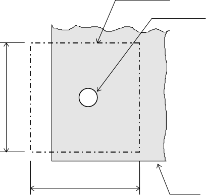
Field of vision for recognizing the PWB reference marks
6.3 mm (camera’s field of vision for recognition).
Figure Field of vision for recognizing the PWB reference marks
Window size for recognizing the PWB reference marks
This size can be changed within a maximum of 6.3 mm, subject to securing a clearance
between the recognition mark and its surrounding area.
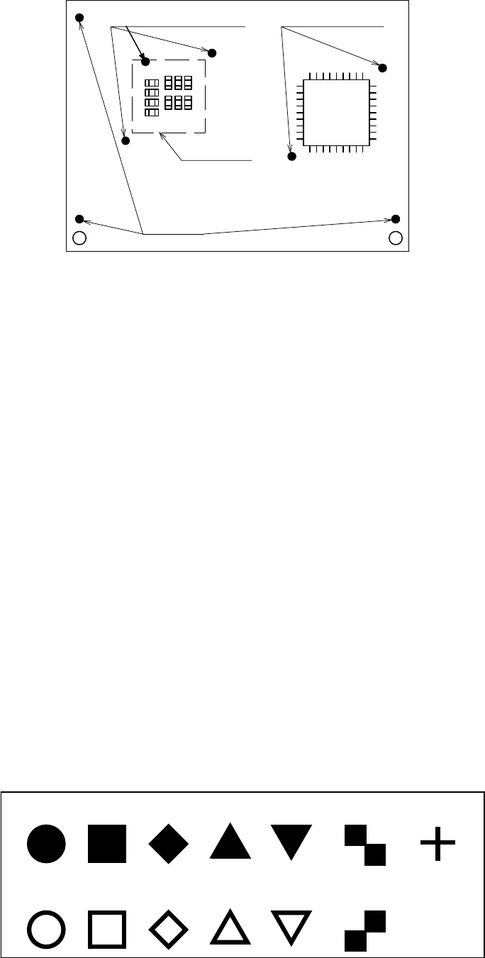
Kinds of recognition marks and corrective method
- PWB reference mark
Two or three marks are located on a PWB to correct the entire PWB.
When the machine detects two PWB reference marks, it corrects the positioning,
angle and expansion/contraction of the entire PWB. When detecting three PWB
reference marks, it corrects the perpendicularity in the X and Y direction also.
- Component positioning marks
If a component such as an IC (QFP) needs to be placed on a board very precisely,
two or three marks set on the component itself are used to correct each component
placement position.
- Marks used to position the component area
Two marks (their positions can be set as you like) are to be provided to a group of
components placement positions, and they are used to correct each component
placement position in the group.
Note 1: You can set a mark at any position. However, if three reference marks are set, they
must not be aligned with one another. (It is recommended that these marks be set at
corners of the board.)
Note 2: When the machine supports feeding of a board whose size exceeds 610 mm
×
360 mm
twice, one set of two or three reference marks is required for each feeding operation
(total four or six marks). When it supports optional feeding of a board whose size
exceeds 1,200 mm
×
360 mm three times, one set of two or three reference marks is
required for each feeding operation (total six or nine marks).
Field of vision for PWBs recognition
Recognition mark
PWB
6.3mm
6.3mm
- 16 -
搭載グループ
エリア部品位置決めマーク 部品位置決めマーク
基準マーク
Figure Reference marks and components positioning marks
Basic quality of recognition marks
- Copper not coated or coated
- It needs to have a clear contrast between the recognition mark surface and the print
wiring quality.
- It needs to have neither oxidation nor quality deterioration of the recognition marks.
Coating the recognition marks
The recognition mark surfaces shall all be coated as follows:
- Transparent antioxidant coating - Solder plating
- Nickel plating - Gold plating
- Tin plating - Hot-air levelling solder coating
Marking forms
- The standard marks represent the thirteen (13) forms as shown in the following
block, “forms of recognition marks.”
- For any mark other than those shown in the said block, customers shall make
templates to allow for recognition through a pattern matching.
Note 1: Limited to the standard marks only
;
and any area fiducial mark is excluded
from the subjects.
Note 2: Within a field of vision, there should be no similar form pattern other than the
subjected form patterns.
- For regular triangles, checker patterns and users’ templates, the 90°up-side-down
marks can also be recognized.
Circle Square Diamond
Regular
triangle
Up-side-down
triangle
Checker
pattern
Cross
Inside-blank
circle
Inside-blank
square
Inside-blank
diamond
Inside-blank
up-side-down
triangle
Checker
pattern
Inside-blank
Regular
triangle
Figure Forms of Recognition Marks
The recognition marks shall all comply with EIAJ ET-7302 “Recognition marks for
on-surface placed PWBs.”
Component placement
area positioning marks
Component positioning
marks
Placement group
PWB reference marks
- 17 -
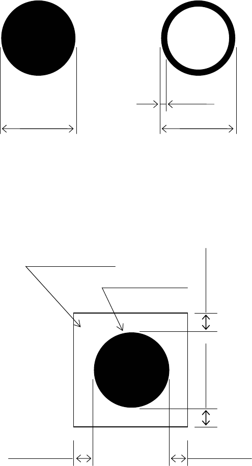
Dimensions and tolerances
The outside dimensions shall range from 0.5 mm up to 3.0mm, whose tolerance, less
than 10%.
For all the inside-blank forms, the edging line width shall be more than 0.2 mm.
Figure Dimensions and tolerances of recognition marks.
It is desirable that there is, around each recognition mark, a space having nothing of such
other marks as conductor pattern, solder resist, marking and the like, and that this space
dimensions is a square than the mark by 0.5 mm or more from the outer circumference of
the recognition marks.
Figure Clearances of recognition marks
0.5 to 3.0mm
0.5 to 3.0mm
0.2 mm or more
Clearance area
Recognition mark
0.5 mm or more
0.5 mm or more
0.5 mm or more
0.5 mm or more