JX-300LED_SPE_EN01.pdf - 第21页
- 17 - Dimensions and tolerances The outside dimensions shall range from 0.5 mm up to 3.0mm, whose tolerance, less than 10%. For all the inside-blank forms, the edging line wid th shall be more than 0.2 mm. Figure Dimens…
- 16 -
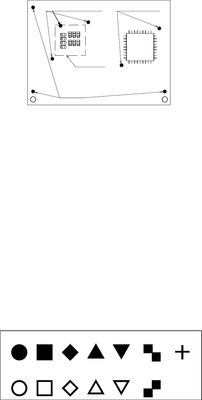
搭載グループ
エリア部品位置決めマーク 部品位置決めマーク
基準マーク
Figure Reference marks and components positioning marks
Basic quality of recognition marks
- Copper not coated or coated
- It needs to have a clear contrast between the recognition mark surface and the print
wiring quality.
- It needs to have neither oxidation nor quality deterioration of the recognition marks.
Coating the recognition marks
The recognition mark surfaces shall all be coated as follows:
- Transparent antioxidant coating - Solder plating
- Nickel plating - Gold plating
- Tin plating - Hot-air levelling solder coating
Marking forms
- The standard marks represent the thirteen (13) forms as shown in the following
block, “forms of recognition marks.”
- For any mark other than those shown in the said block, customers shall make
templates to allow for recognition through a pattern matching.
Note 1: Limited to the standard marks only
;
and any area fiducial mark is excluded
from the subjects.
Note 2: Within a field of vision, there should be no similar form pattern other than the
subjected form patterns.
- For regular triangles, checker patterns and users’ templates, the 90°up-side-down
marks can also be recognized.
Circle Square Diamond
Regular
triangle
Up-side-down
triangle
Checker
pattern
Cross
Inside-blank
circle
Inside-blank
square
Inside-blank
diamond
Inside-blank
up-side-down
triangle
Checker
pattern
Inside-blank
Regular
triangle
Figure Forms of Recognition Marks
The recognition marks shall all comply with EIAJ ET-7302 “Recognition marks for
on-surface placed PWBs.”
Component placement
area positioning marks
Component positioning
marks
Placement group
PWB reference marks
- 17 -
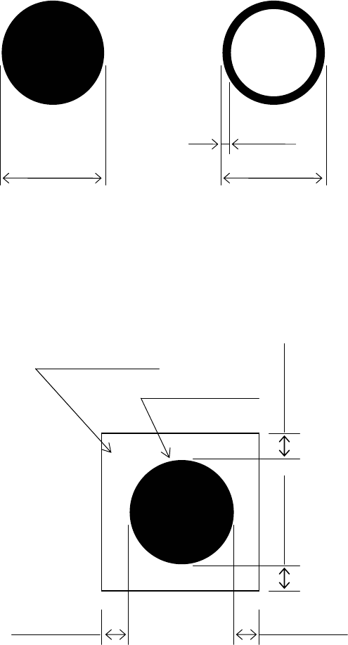
Dimensions and tolerances
The outside dimensions shall range from 0.5 mm up to 3.0mm, whose tolerance, less
than 10%.
For all the inside-blank forms, the edging line width shall be more than 0.2 mm.
Figure Dimensions and tolerances of recognition marks.
It is desirable that there is, around each recognition mark, a space having nothing of such
other marks as conductor pattern, solder resist, marking and the like, and that this space
dimensions is a square than the mark by 0.5 mm or more from the outer circumference of
the recognition marks.
Figure Clearances of recognition marks
0.5 to 3.0mm
0.5 to 3.0mm
0.2 mm or more
Clearance area
Recognition mark
0.5 mm or more
0.5 mm or more
0.5 mm or more
0.5 mm or more
- 18 -
5. Standard Functions And Optional Functions
5.1 Standard Functions
5.1.1 Support up to 1,200 mm as the X axis of a board
When the X dimension of a board is 610 mm or less, the machine clamps it once to
transport it. When it exceeds 610 mm but it is 1,200 mm or less, the machine clamps it
twice to transport it. In this way, the machine can produce a PWB whose size is up to
1,200 mm that is to be used in a LED light.
The whole length of the board transport path is 1,920 mm.
5.1.2 Feeder float detecting sensor (Front side only)
This function is provided to prevent mechanical troubles caused by improper installation
of tape or stick feeders. When this sensor detects an improperly-installed feeder, it
stops the X-Y axes, and warns an operator.
5.2 Optional Functions
5.2.1 Height Measurement System (HMS) (Factory-set option)
When preparing the pick data, the component pick position and height shall all be
measured via the laser sensors. Components (for example, LEDs) whose pick surface is
transparent such as glass and a substance in a mirror state from which the light is fully
reflected, blue components shall all be excluded from the subjects of the HMS. The
HMS is used to set a teaching spot also.
5.2.2 Bad mark reader (Factory-set option)
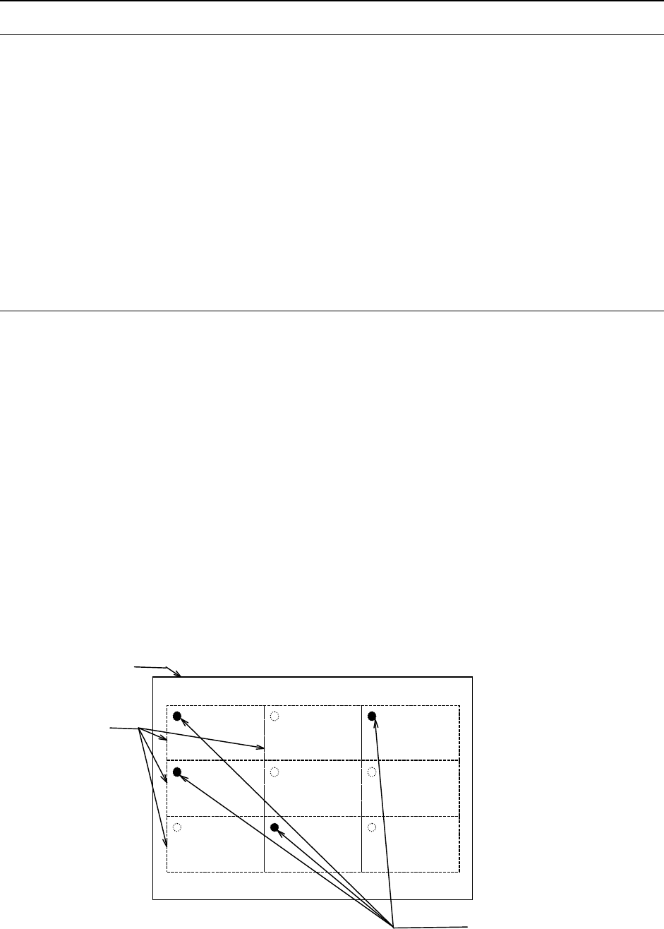
A bad mark is given to a circuit on a multi-circuit PWB to prevent any component from
being placed on the circuit.
The minimum diameter of a bad mark is 2.5 mm or more and the color of a mark should
be highly contrasted with the color of a board. The brightness can be switched when the
color of a board is bright (looks white).
When you use an optional bad mark reader, the time for recognizing one bad mark can
be shortened by approximately 0.1 seconds with comparing with the time taken with the
standard OCC camera.
Figure Bad marks
Circuit
Board
Bad marks