HF Circuit .pdf - 第193页
4 - 6 0036554 4-020 201ZD3 Control com plete, P CB d ual con veyor (Sh . 2 of 2 ) A Stat us Modifi ed Date Nam e Ori g. Stand. Date Aut hor Check. Repl. by Repl. f. 2 2 Drawing 00 343603-xx Ground connection Label 2 Labe…
4 - 5
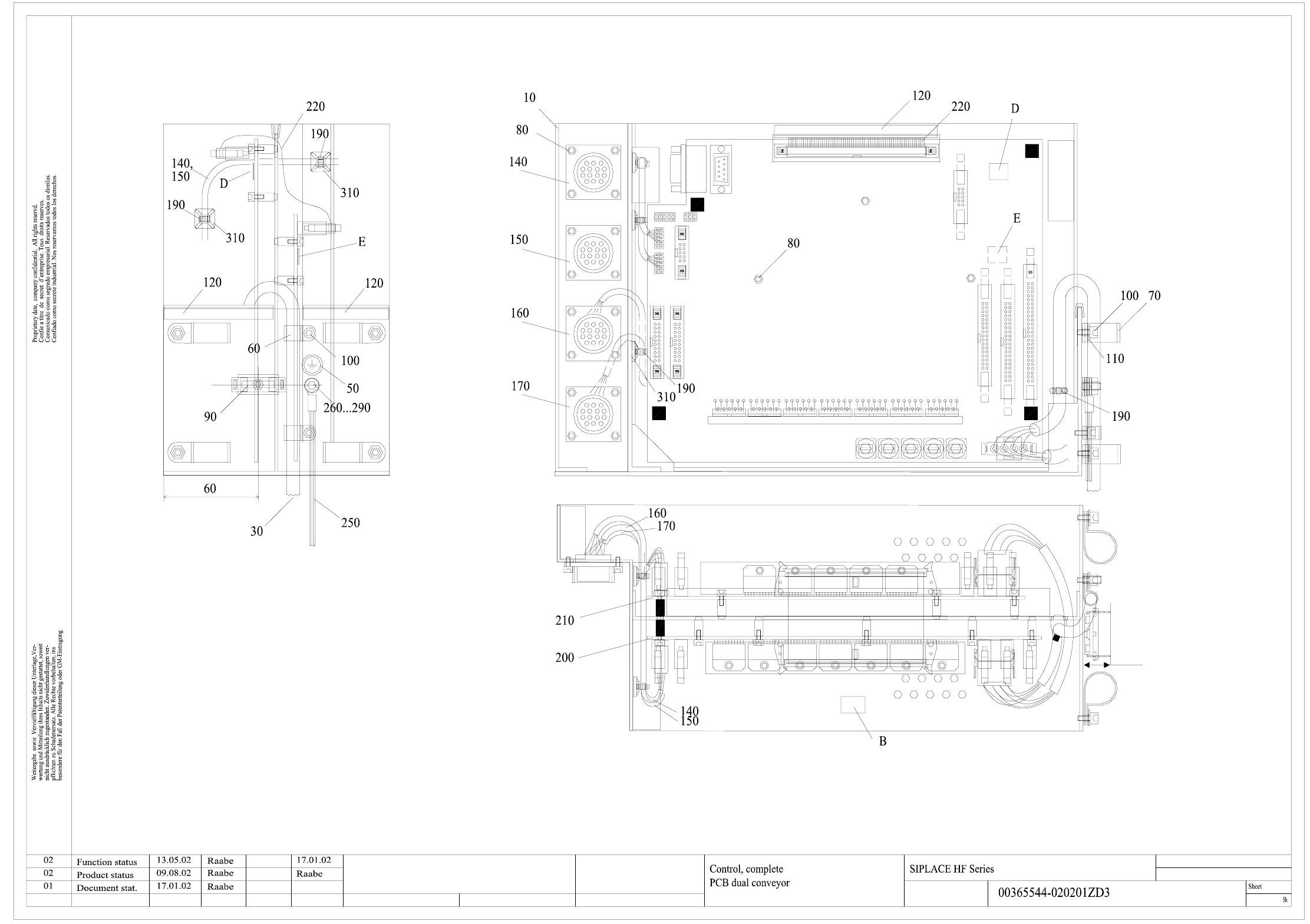
00365544-020201ZD3 Control complete, PCB dual conveyor (Sh. 1 of 2)
Stand.
Check.
Author
Date
Status
Modified Date Name
Orig. Repl. f.
B
D
E
Repl. by
2
1
Ground connection
Drawing 00343603-xx
Space for inspection label
Label for module identification "ao"
Label for module identification "ap"
To be shortened
to 20+/-3mm
A&D EA
s
4 - 6
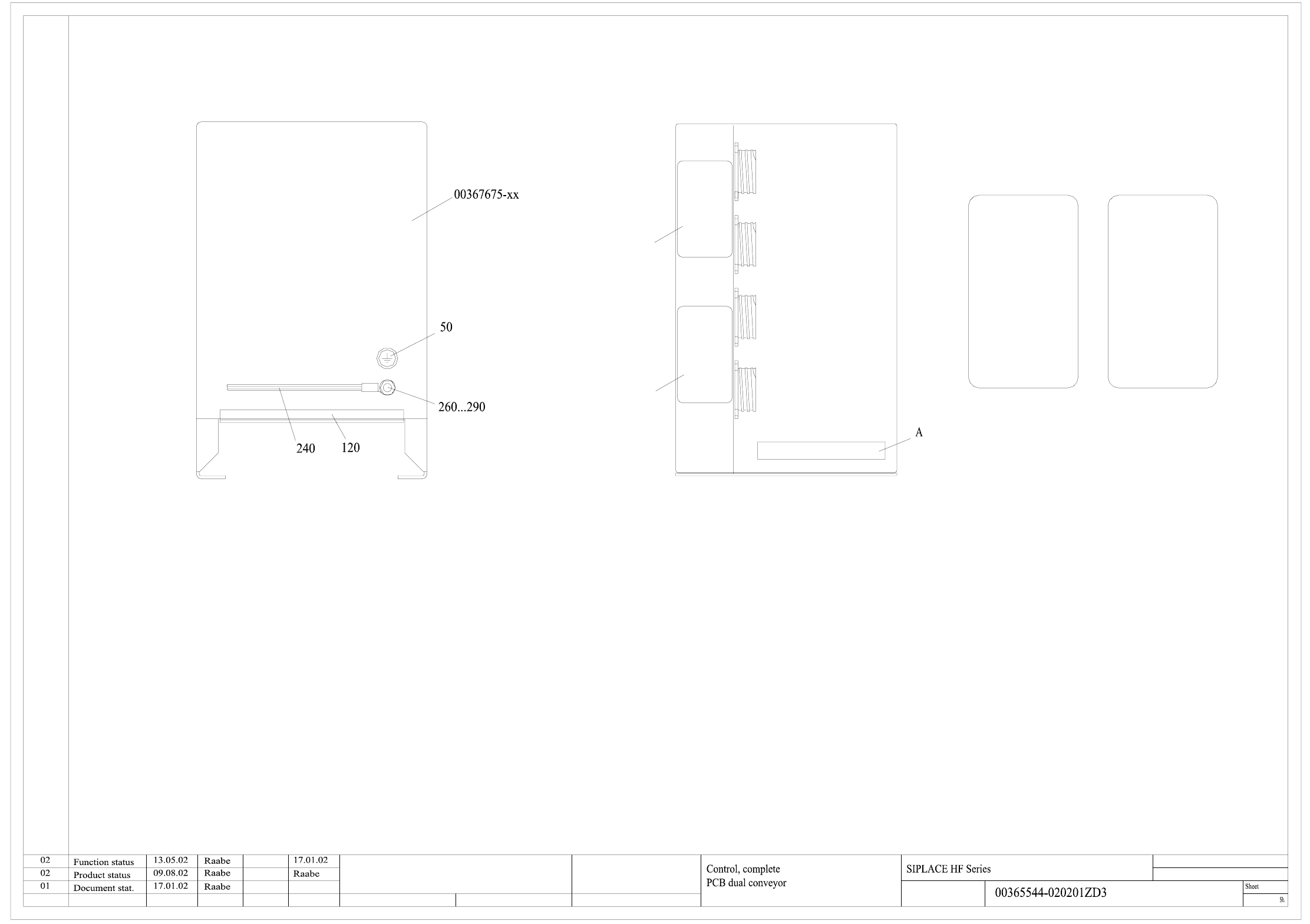
00365544-020201ZD3 Control complete, PCB dual conveyor (Sh. 2 of 2)
A
Status Modified Date Name
Orig.
Stand.
Date
Author
Check.
Repl. byRepl. f.
2
2
Drawing 00343603-xx
Ground connection
Label 2
Label 1
upstream station
downstr. station
SMEMA Interface
Spur 1 / track 1
Nachfolger/
Vorgänger/
upstream station
Vorgänger/
Nachfolger/
downstr. station
SMEMA Interface
Spur 2 / track 2
Space for identification label
Label 1 Label 2
downstr. station
Nachfolger/
SMEMA Interface
Spur 2 / track 2
Vorgänger/
upstream station
SMEMA Interface
Spur 1 / track 1
upstream station
downstr. station
Nachfolger/
Vorgänger/
Confiado como secrete industrial. Nos reservamos todos los derechos.
Comunicado como segredo empresarial. Reservados todos os direitos.
Confie a titre de secret d'entreprise. Tous droits reserves.
Proprietary date, company confidential. All rights reserved.
Weitergabe sowie Vervielfältigung dieser Unterlage,Ver-
wertung und Mitteilung ihres Inhalts nicht gestattet, soweit
nicht ausdrücklich zugestanden. Zuwiderhandlungen ver-
pflichten zu Schadenersatz. Alle Rechte vorbehalten, ins
besondere für den Fall der Patenterteilung oder GM-Eintragung
A&D EA
s
4 - 7
03010004-030101TD1 Main distributor
DI12 -
DI8 -
DI7 -
DI6 -
DI5 -
DI4 -
DI1 -
34
33
32
31
30
29
28
27
1
X17qa
X23qa
X24qa
X18qa
X21qa
X20qa
X19qa
X22qa
X74qaX2qaX3qaX4qaX5qaX6qaX9qa X72qa X71qaX73qaX10qaX11qaX12qaX13qaX14qaX16qa
A
B
2
3
4
5
6
7
8
9
10
11
12
13
14
15
16
17
18
19
20
21
22
23
24
25
26
X74qaX2qaX3qaX4qaX5qaX6qaX9qa X72qa X71qaX73qaX10qaX11qaX12qaX13qaX14qaX16qa
X17qa
X23qa
X24qa
X18qa
X21qa
X20qa
X19qa
X22qa
X1qa
DI19 - S_HoodPCBOutput
DI17 - S_Hood2
DI18 - S_COtable2
DI16 - S_EmergStopLoop2Ok
DI21 - S_Hood3
DI22 - S_COtable3
DI20 - S_EmergStopButtonPCBOutput
DO14 - Ctrl_FaultIndLamp2
DO12 - Ctrl_GreenLamp1
DO13 - Ctrl_FaultIndLamp1
DO15 - Ctrl_GreenLamp2
DI23 -
DI9 - S_Ready
DI15 - S_PressureSensor C&P/TWIN
DI13 - S_ControlOn
DI10 - S_PressureSensor C&P20
DI11 - S_GantryCrash1
DI3 - S_Flap
DI0 - EmergStopLoopOk
LEDs on the CAN I/O module
DO3 - Ctrl_ComprAir C&P/TWIN
DO1 - SoftwareRelease
DO2 - Ctrl_ComprAir C&P20
DO4 - Ctrl_COcounter
DO6 -
DO7 -
DO8 -
DO9 -
DO10 -
DO11 -
DO0 -
DO5 -
DI2 -
DI14 -
PE
X15qa
X15qa
B: Inspection label Identification: Test. engineer, month, year
A: Identification label
* Note
Apply the following labels on the assembly:
Meaning
CAN-Error Switch
no CAN terminator
ON:OFF
CAN group = 0
CAN-Speed = 500 kbit/s
ID0
ID1
CAN-Error Switch
Boot
Reset OFF
Switch
S1.1
Setting
ID1
ID0
CAN-Speed = 1 Mbit/s
CAN group = 1
S1.2
S1.3
S1.4
S1.5
S1.6
S1.7
S1.8
CAN terminator 120 Ohm OFF
OFF
OFF
OFF
OFF
Switch S1 on the vision control unit
SW 504:
SW 505 and later:
S1 switch on the CAN I/O module
OFF
not used
not used
Main distributor
Sub-distributor
OFF
ON:
OFF: SIPLACE X series
SIPLACE HF, HF/3
OFF
OFF
ON
OFF
OFF
not used
not used
1-wire PC
not used
not used
not used
1-wire MA
not used
I/O module
Slio emulation
1000k
500k
Terminating resistor
CAN
not used
1-Wire
not used
Location
Location
Platform
Baud rate
S1.8
S1.7
S1.6
S1.5
S1.4
S1.3
S1.2
OFF:
ON:
OFF:
ON:
OFF:
ON:
OFF:
ON:
OFF:
ON:
OFF:
ON:
OFF:
ON:
OFF:
ON:
SettingCodingMeaning
S1.1
Switch
ON
OFF
SW 504:
SW 505 and later:
OFF
ON
A5 (qe)
8x
'AND gate
123123 87654
X1qe
X3qe
X2qe
K2
DO8
DO0
DO0
DO15
LEDs
LEDs
VCC
GND
EGND
EGND
DI4_5V
DI5_5V
DI6_5V
DI7_5V
12345678
X6qb
DI16
12345678
X5qb
1234567812345678
X4qb X3qb
DI17
DI18
DI19
DI20
DI21
DI22
DI23
DI8
DI9
DI10
DI11
DI12
DI13
DI14
DI15
DI0
DI1
DI2
DI3
DI4
DI5
DI6
DI7
DO10
X7qbX8qb
12345678
P24
GND
X9qb
12345678
12345678
DO0
DO1
DO2
DO3
DO4
DO5
DO6
DO7
P24
P24
P24
GND
GND
GND
DO11
DO12
DO13
DO14
DO15
DO8
DO9
X2qb
X1qb
X10qb
S1
S1.8:
01
ON="1"
OFF="0"
S1.7:
S1.6:
S1.5:
S1.4:
S1.3:
S1.2:
S1.1: Baud rate
Platform
Location
Location
not used
1-Wire
not used
Terminating resistor
CAN I/O module
A1 (qb)
DI0
DI7
DI8
DI15
DI16
DI23
K1
Vision control 1 assy
A4 (qd)
12345678
ON
X8qd
X4qd X5qd
X9qd
X7qd
X6qd
X1qd
X2qd
X3qd
S1
X2qc
19 20 21 22 23 24 25 26
X3qc
X5qc
X4qc
X6qc
1817
45678910
161514
321 111213
8
4
765
321
X1qc
Vision DC/DC converter
A3 (qc)
16
12345678910111213141516
123456789101112131415
A
B
C
D
E
F
G
H
I
K
A
B
C
D
E
F
G
H
I
K
SIPLACE HF series
Main distributor
03010004-030101TD1
Drawing no. (FS RS DS DT L F)
Klein H.08.08.2003
Modified / ECO no.
K4, K5 no longer usedFS02
ECR no.
FS03 400870
Siemens AG
06.06.2005
Name
Tek
Date
06.02.04
Tek06.06.05
Author
Stand.
Check.
A&D
Repl. f.
Date
ISO 2768 mH, unless
General tolerances
for nominal dimensions as per
otherwise specified
Degree of accuracy
DIN 7167
Name
Material
Scale
1Sh.
1
Sheet
Format
A1
Weitergabe sowie Vervielfältigung dieser Unterlage, Verwer-
tung und Mitteilung ihres Inhalts nicht gestattet, soweit nicht
ausdrücklich zugestanden. Zuwiderhandlungen verpflichten zu
Schadenersatz. Alle Rechte für den Fall der Patenterteilung
oder GM-Eintragung vorbehalten.
Copying of this document, and giving it to others and the use
or communication of the contents thereof, are forbidden with-
out express authority. Offenders are liable to the payment of
damages. All rights are reserved in the event of the grant of
a patent or the registration of a utility model or design.