HF Circuit .pdf - 第256页
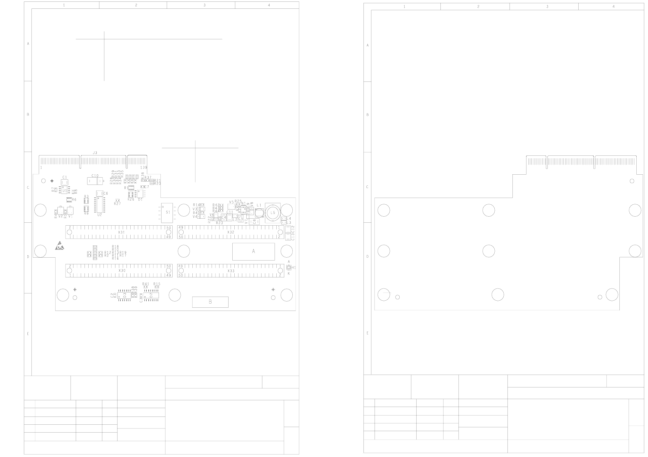
5 - 47 03002116-010101N D1 KSP-SYSS0 1 03002116-010101 ND1 b) Position for inspectio n label on side 1 a) Position for identification label on side 1 Dashe d li nes in dica te th at components are to be placed on side 2 …
5 - 46
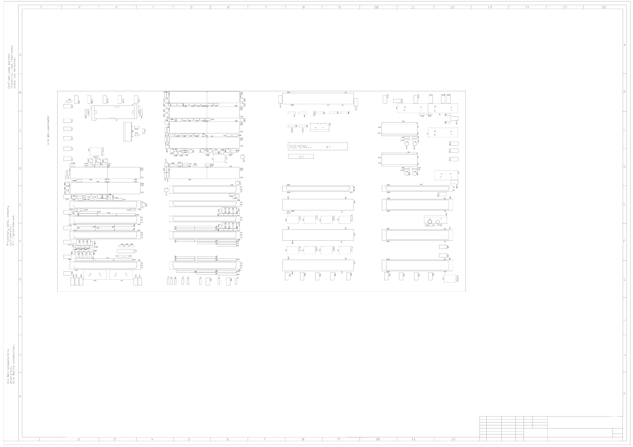
03000902-030101ND4 PCB 995, head adapter P&P (Sh. 1 of 2)
03000902-030101ND4 PCB 995, head adapter P&P (Sh. 2 of 2)
(G32918-N0047-U041-*)
Proprietary data, company confidential. All rights reserved.
Confie a titre de secret d'entreprise. Tous droits reserves.
Confiado como secrete industrial. Nos reservamos todos los derechos.
Stat.
04
01
03
02
Modified
--------
--------
--------
--------
13.04.04
14.06.02
11.02.02
11.07.01
Date
EN
KL
KL
KL
Name
EDM E MCH
SIEMENS
Date
Name
11.07.01
Klose
03000902-030101ND4
A2B00039786C-U041-*-ZEI
P&P head adapter
Component layout, component side
SIPLACE HF series
Board 995
4-layer PCB
Sc 1:1
1 +
Sheet
A = Identification label
B = Inspection label
Only insert either L1 or L5.
X31 head main board C600, 00352833, P&P module 2
X30 head main board C600, 00352833, P&P module 2
X22 head interface, 03000901
X31 head main board C600, 00352833, P&P module 1
X30 head main board C600, 00352833, P&P module 1
X33
Assembly
X31
X32
X30
J3
Connector
1
2
4
3
Switch S1
0
0
0
0
Gantries 1 and 3
Comunicado como segredo empresarial. Reservados todos os direitos.
pflichten zu Schadenersatz. Alle Rechte vorbehalten, ins
besondere für den Fall der Patenterteilung oder GM-Eintragung
wertung und Mitteilung ihres Inhalts nicht gestattet, soweit
Weitergabe sowie Vervielfältigung dieser Unterlage,Ver-
nicht ausdrücklich zugestanden. Zuwiderhandlungen ver-
ModifiedStat.
01
02
03
04
--------
--------
--------
--------
EDM E MCH
NameDate
13.04.04
14.06.02
11.02.02
28.06.01
EN
KL
KL
KL
SIEMENS
Name
Date 28.06.01
Klose
A2B00039786C-U041-*-ZEI
03000902-030101ND4
(G32918-N0047-U041-*)
P&P head adapter
Component layout, solder side
SIPLACE HF series
Board 995
4-layer PCB
Sc 1:1
2 -
Sheet
2
Confiado como secrete industrial. Nos reservamos todos los derechos.
Comunicado como segredo empresarial. Reservados todos os direitos.
pflichten zu Schadenersatz. Alle Rechte vorbehalten, ins
besondere für den Fall der Patenterteilung oder GM-Eintragung
wertung und Mitteilung ihres Inhalts nicht gestattet, soweit
Weitergabe sowie Vervielfältigung dieser Unterlage,Ver-
nicht ausdrücklich zugestanden. Zuwiderhandlungen ver-
140
Proprietary data, company confidential. All rights reserved.
Confie a titre de secret d'entreprise. Tous droits reserves.
5 - 47
03002116-010101ND1 KSP-SYSS01
03002116-010101ND1
b) Position for inspection label on side 1
a) Position for identification label on side 1
Dashed lines indicate that
components are to be placed on side 2
Modified
Fan
View onto side 1
Pressfit technology
L&A EA - document number:
NameStat. Date
Schu19.11.015547/1A1
5547/2B1 Schu06.02.02
WKF - B10.53
SIEMENS
AG
Placement diagram, page 1
J31070-A5547-A001-B1-0017
KSP-SYSS01
Sheet
Sh.1
1
19.11.01
Schusser
Check.
Stand.
Author
Date
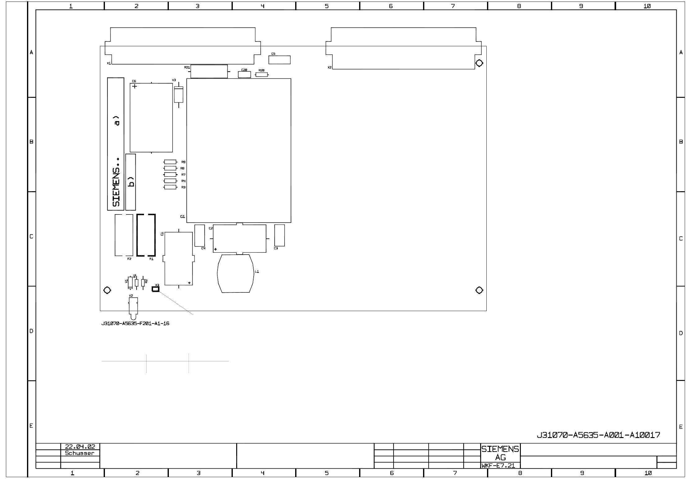
5 - 48
03002126-030101ND3 Power supply 24V/3.3V
03002126-030101ND3
A1 A5635/1 13.02.03 Schu
a) Location for identification label
24V/3.3V (UL) POWER SUPPLY
V2
LED
3.3V
X3: 3.3V test socket
F1: 2AT/250V slow-blow fuse
F1
X3
green
Sh. 1
Sh. 1
Name
Stat. Modified Date
Confiado como secrete industrial. Nos reservamos todos los derechos.
Proprietary data , company confidential . All rights reserved.
Confie a titre de secret d'entreprise. Tous droits reserves.
Comunicado como segredo empresarial. Reservados todos os direitos.
b) Location for inspection label
Check.
Author
Date
Stand.
besondere fuer den Fall der Patenterteilung oder GM-Eintragung.
nicht ausdruecklich zugestanden. Alle Rechte vorbehalten, ins-
wertung und Mitteilung ihres Inhalts nicht gestattet, soweit
Weitergabe sowie Vervielfaeltigung dieser Unterlage, Ver-
Components with axial leads, side 1
Placement diagram
Bauteilangaben nur zur Information