presto_en.pdf - 第21页
Page 21 4) The safety fuse on the JTAG interface can not be blown by the PRESTO programm er. 5) The HPR3V3 adapt er sho uld be used for feeding these microcont rollers (with out the SBW int erface) from PRESTO in ternal …
Page 20
1) The SS pin must be connected only for AT89LP2052 /
4052 / 213 / 214 / 216 / 428 / 828 / 6440 / 51RD2 /
51ED2 / 51ID2 / 51RB2 / 51RC2 / 51IC2.
2) AT89LP213, AT89LP214 and AT89LP216 have the
inverse reset logic. Thus an appropriate resistor must
be pulled-up to VCC.
3) PRESTO can not program devices containing the
letter “C” in their name, however, it supports devices
with “S” in their name, of which some are compatible
with the “C” types. For example, AT89C2051 is not
supported, but AT89S2051 is.
4) The software assumes that while programming
AT89LP52, the device’s POL pin is in logical1. If POL
is in logical0, the Inverse RESET option should be
activated in the program. For AT89LP51RD2,
AT89LP51ED2, AT89LP51ID2, AT89LP51RB2,
AT89LP51RC2 and AT89LP51IC2 the software
assumes the POL pin in logical0.
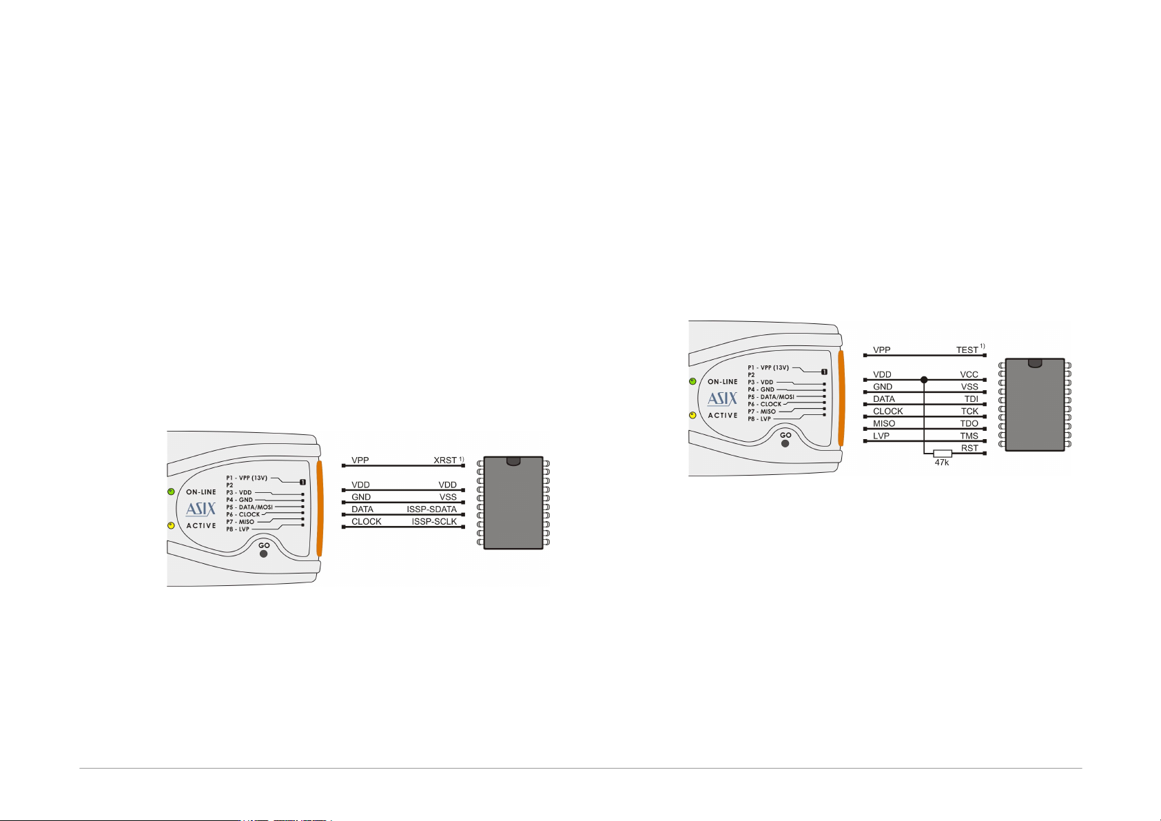
Cypress PSoC
Fig.10: Cypress PsoC microcontroller
1) The way of entering in the programming mode
should be set in the PRESTO programmer settings
window. Devices without an XRST pin can only use
initialization through the power-on reset (by power
supply). Devices with an XRST pin may use both
methods, but the method using the reset signal for
initialization is better as it can be used in
combination with an external power supply.
2) Algorithm programming in the PRESTO
programmer settings window should be set in
accordance with the power supply cable used.
MSP430 with TEST pin without
SBW interface
Fig.11: MSP430 microcontroller, TEST pin, without SBW
1) Not all MSP430 microcontrollers have the TEST pin.
2) This interconnection can be used with e.g.
MSP430F1xx, MSP430F4xx, MSP430F21x1, but not
with MSP430F20xx or MSP430F22xx.
3) If the oscillator calibration values are saved in the
information memory and this memory is not going to
be re-programmed (erased) during programming, the
device should be programmed with the Cal Int. RC
(=calibrated internal RC oscillator) option selected in
the PRESTO programmer settings window. In the
other cases Not Cal Int. RC (=not calibrated internal
RC oscillator) should be selected.
Page 21
4) The safety fuse on the JTAG interface cannot be
blown by the PRESTO programmer.
5) The HPR3V3 adapter should be used for feeding
these microcontrollers (without the SBW interface)
from PRESTO internal 5V power supply.
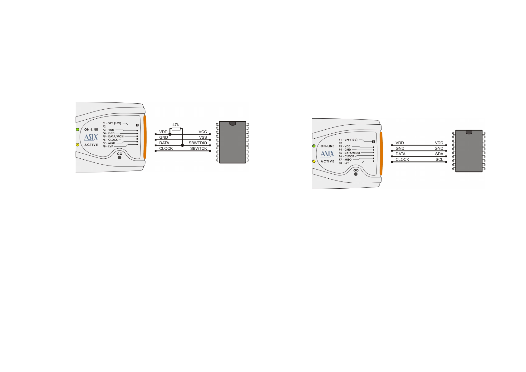
MSP430 / CC430 with SBW
interface
Fig.12: MSP430 / CC430 microcontroller, SBW
1) Microcontrollers with SBW interface could be
programmed only through this interface. It concerns
e.g. MSP430F20xx, MSP430F22xx or MSP430F5xxx.
2) If the oscillator calibration values are saved in the
information memory and this memory is not going to
be re-programmed (erased) during the programming
process, the device should be programmed with the
Cal Int. RC (=calibrated internal RC oscillator)
option selected in the PRESTO programmer
settings window. In the other cases Not Cal Int. RC
(=not calibrated internal RC oscillator) should be
selected. There is no need to select the oscillator for
the MSP430F5xxx and CC430 devices.
3) The safety fuse on the JTAG interface cannot be
blown by the PRESTO programmer.
4) Speed in the PRESTO programmer settings
window should be slow down if any external
capacitor is connected to the device's reset pin.
5) The PRESTO programmer also erases the Segment A
of the information memory with the
EraseSegmentA option selected.
TI (Chipcon) CCxxxx
<<( ti_chipcon.jpg | 10cm | TI (Chipcon) Ccxxxx
microcontroller )
I2C Memory Chips
Fig.13: I2C memory chips
1) The programmer uses an internal 2.2kΩ pull-up
resistor on the data wire (SDA) when working with an
I2C device.
2) If the device to be programmed is 24LC(S)21A or
24LC(S)22A, its VCLK pin must be connected to VDD
during programming.
3) 34xx02 memory chips need “high” voltage at the A0
pin for commands protecting it against SWP and
CSWP recording. The “high” voltage is generated at
pin P, which must be connected to pin A0 in this
case. The memory chip pins A0, A1 and A2 must be
connected manually according to the selected
protection mode.
Page 22
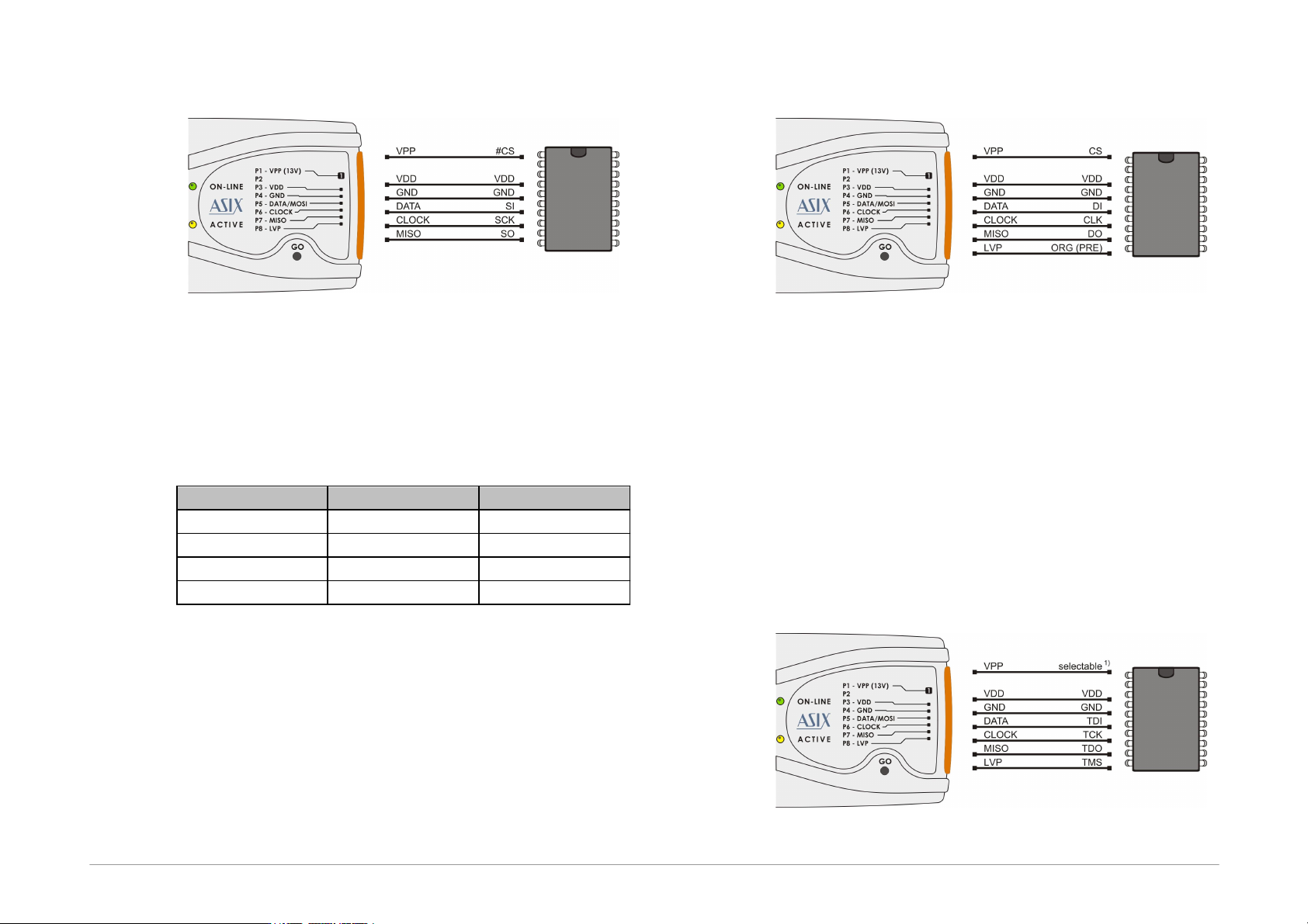
SPI Memory Chips
Fig.14: SPI memory chips
1) Some devices have WP, HOLD or RESET pins. All of
them must be connected to the required logic level in
such a way as not to block the communication or
device programming.
2) Different manufacturers mark the memory chips' SPI
pins with different names. Some of them are listed in
the following table:
Name on figure
Atmel, SST
ST
DI
SI
D
DO
SO
Q
CLK
SCK
C
#CS
CS, CE
S
3) The HPR3V3 adapter should be used for feeding SPI
memory chips from PRESTO internal 5V power
supply.
Microwire Memory Chips
Fig.15: Microwire memory chips
1) Pin L determines the memory organization as either
8-bits or 16-bits per word. The user selects the
required organization in the UP program and PRESTO
then sets this pin to the corresponding logic level. If
this memory pin is firmly connected to the correct
logic level inside the application, pin L in the
programmer remains disconnected.
2) If used in combination with the M93Sx6 memory chip,
the programmer's L pin must be connected to the
device's PRE pin to serve for selecting the protection
register.
JTAG Interface
Fig.16: Components with JTAG interface