presto_en.pdf - 第81页
Page 81 Notes • An error may occur if UP cannot program the calibration word or if a fault oc curs during Device ID reading, UP warns about an o vercurrent at VDD, etc. This may be eliminated by prolong ing the charg ing…
Page 80
maximum load is substantially exceeded for a certain
time (this time is adjustable). PRESTO checks for the
overload state the whole time the power supply is
connected.
Support for an external power supply is integrated in both
PRESTO and FORTE hardware. The programmer feeds the
input and output circuits with a voltage connected to pin
VDD. The voltage may be lower than 5V.
Advice
When designing the process, please pay special attention
to the type of device to be programmed – if it can be not
only operated but also programmed at a voltage lower
than 5V.
Power Supply Capacities in
Application
If there are capacities present at the application's power-
supply pin that would slow down the power on/off
switching and application is fed from programmer during
programming, longer charging/discharging times need to
be set in UP. In other case UP will probably announce
overcurrent on VDD pin.
An approximate time that should be set in the program:
t[μs] = 2.5 × C[μF] × R[Ω].
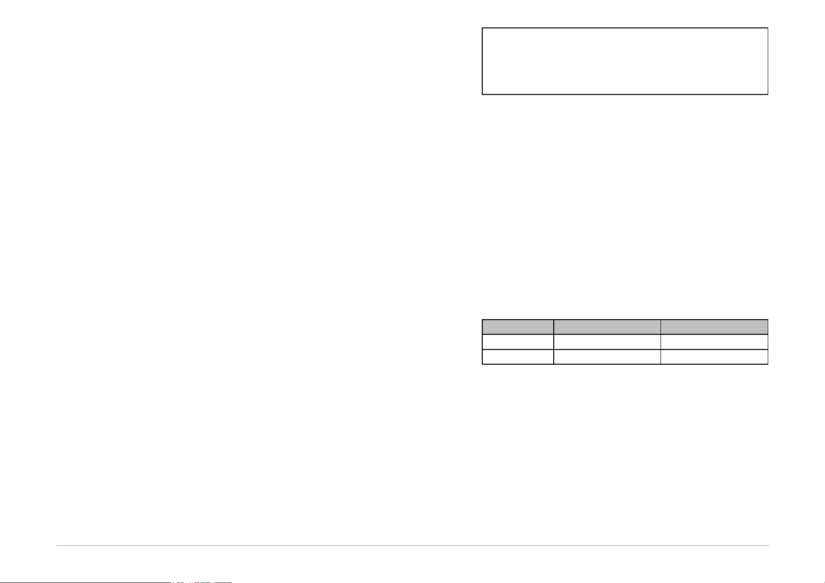
The equivalent resistance is presented in table following
table:
Programmer
Charging current
Discharging current
PRESTO
Corresponds to 50Ω
Corresponds to 1kΩ
FORTE
Corresponds to 50Ω
Corresponds to 27Ω
Table10: Equivalent resistance of pin VDD
Example
The necessary charging time for an application with
a33μF capacitor programmed with PRESTO:
2.5×33×50=4125μs
discharging:
2.5×33×1000=82.5ms.
For further information on the setting see
▸ Delay for VDD
switching on/off when supplied from programmer.
Page 81
Notes
• An error may occur if UP cannot program the
calibration word or if a fault occurs during Device ID
reading, UP warns about an overcurrent at VDD, etc.
This may be eliminated by prolonging the charging/
discharging time in the
▸ Delay for VDD switching on/
off when supplied from programmer
option - up to
several seconds.
• If UP points out an overcurrent error at VPP, a shorter
ICSP cable may help (its maximum length is 15cm).
5.13.3 ICSP Connector
All ASIX programmers use a unified connector with
2.54mm spacing of pins for programming with the ICSP
algorithm.
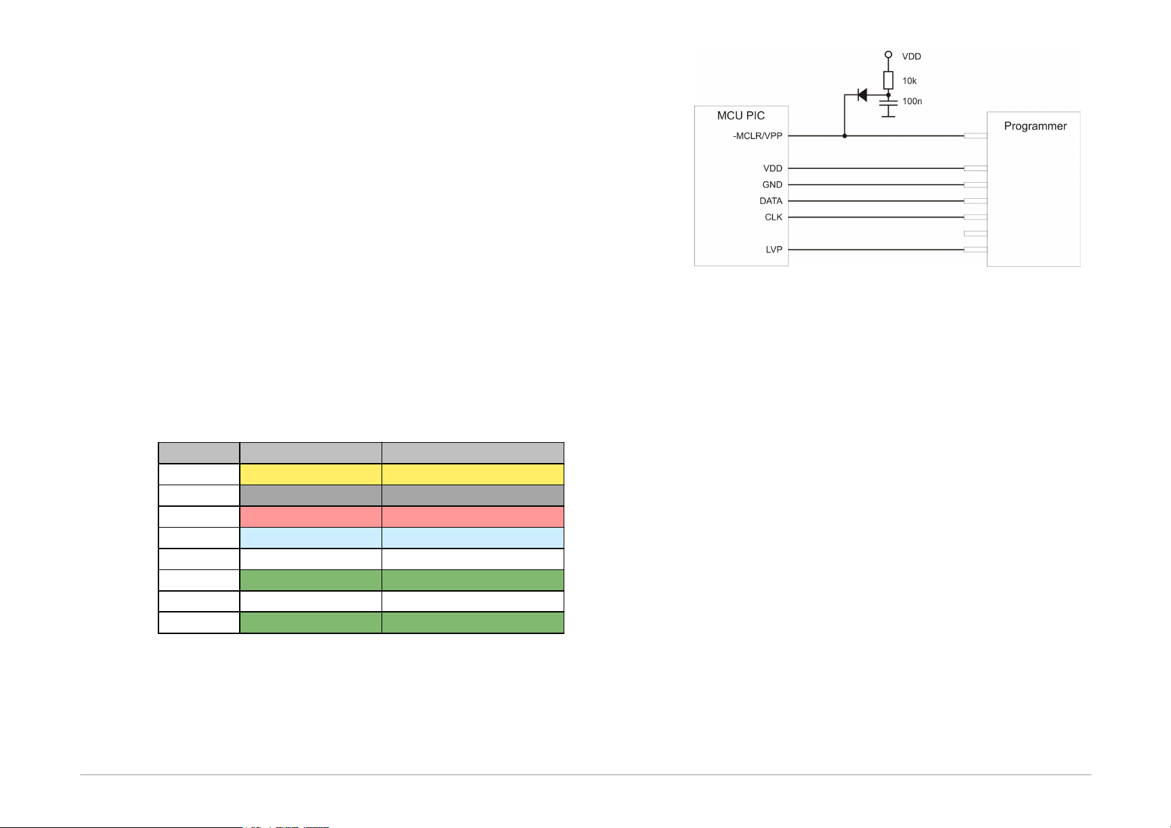
This connector has 8pins with 7signals. Not all signals
are always needed for the programming itself.
For further information on connecting a device to the
programmer see Connection Examples.
Pin No.
Signal
Programming connector
1
-MCLR
P / VPP
2
not used (key)
3
VCC
VDD
4
GND
GND
5
RB7
D / DATA
6
RB6
C / CLOCK
7
not used
8
RB3/RB4/RB5
L / LVP
Table11: ICSP connector
The following drawing illustrates the recommended
connection of -MCLR/VPP pin found in Microchip
microcontrollers for device programming through the
ICSP interface.
Fig.26: Recommended connection of -MCLR/VPP pin
5.14
Appendix C: Intel‑HEX
File Format
This appendix describes the format of Intel-HEX files used
by UP for data reading and saving. .hex is the typical
extension for such a file.
5.14.1 Supported
Alternatives of HEX
Files
UP supports 2 basic alternatives of Intel-HEX files:
• "basic", sometimes also 8-bit Intel-HEX File (e.g.
Microchip MPASMWIN generates this file with
parameter INHX8M).
• "extended", sometimes also 32-bit Intel-HEX File (e.g.
Microchip MPASMWIN generates this file with
parameter INHX32).

Page 82
5.14.2 Description of
Intel‑HEX File Format
Intel-HEX are text files consisting of lines.
Each line has the following structure:
:LLAAAATTDDDD...CC
„:“ Each line in a file must start with this
character (colon, 0x3A).
LL Length of record (number of DD fields).
AAAA Address of record's first byte.
TT Record type. The types may be:
00 - Data
01 - End of file. Each file must finish with
this record.
02 - Extended segment address. (32-bit
Intel-HEX only)
04 - Extended linear address. (32-bit
Intel-HEX only)
There are also other types like 03 and 05, which are
ignored by UP while reading and not used for saving.
DD Record data. The number of bytes must be
exactly LL.
CC Checksum. The check sum is computed as
a binary supplement to the sum of all
values on the line.
Data Record
A line with the configuration memory of a 14-bit device is
used here as an example.
:02400E00413F30
02 Record length. The configuration memory
size is one word = 14 bit = 2 byte (byte
alignment).
400E Record address. The configuration memory
address is the word 2007h addressed by
bytes, i.e. 400Eh.
00 Record type = data
413F Record data. Configuration word =3F41h
30 Check sum. 30 = 02 + 40 + 0E + 00 + 41
+ 3F = xxD0; neg D0 = 30
End of File
The only acceptable alternative of the End of file line is:
:00000001FF
Extended Linear Address
Only files that need to address more than 64 kB of the
addressed space contain this line.
For example, processors of the PIC18F family have their
configuration memory saved at the address 0x 30 00 00
00.
If this address needs to be used, it is necessary to insert a
line in the .hex file specifying the extended linear
address, i.e. the upper 16 bites of the address. The lower
16 bits are read from the line with the data record.
:020000040030CA
This line selects the configuration memory of PIC18F
family devices.
The extended segment records specify the segment, i.e.
bits 19-4 of the address, which are then added to
addresses from the data records (offset).