presto_en.pdf - 第23页
Page 23 1) Pin P is c onfigurable in the JTAG Player utility. It can be set to keep the device in reset durin g programming. This is needed for Atmeg a devices, for example. 2) The programmer always uses an ext ernal pow…
Page 22
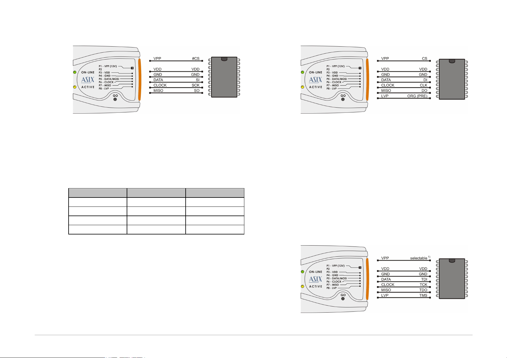
SPI Memory Chips
Fig.14: SPI memory chips
1) Some devices have WP, HOLD or RESET pins. All of
them must be connected to the required logic level in
such a way as not to block the communication or
device programming.
2) Different manufacturers mark the memory chips' SPI
pins with different names. Some of them are listed in
the following table:
Name on figure
Atmel, SST
ST
DI
SI
D
DO
SO
Q
CLK
SCK
C
#CS
CS, CE
S
3) The HPR3V3 adapter should be used for feeding SPI
memory chips from PRESTO internal 5V power
supply.
Microwire Memory Chips
Fig.15: Microwire memory chips
1) Pin L determines the memory organization as either
8-bits or 16-bits per word. The user selects the
required organization in the UP program and PRESTO
then sets this pin to the corresponding logic level. If
this memory pin is firmly connected to the correct
logic level inside the application, pin L in the
programmer remains disconnected.
2) If used in combination with the M93Sx6 memory chip,
the programmer's L pin must be connected to the
device's PRE pin to serve for selecting the protection
register.
JTAG Interface
Fig.16: Components with JTAG interface
Page 23
1) Pin P is configurable in the JTAG Player utility. It can
be set to keep the device in reset during
programming. This is needed for Atmega devices, for
example.
2) The programmer always uses an external
power-supply voltage for SVF or XSVF file
programming by means of the JTAG Player
utility.
3) ARM microcontrollers can be programmed and
debugged through JTAG interface. The ARMINE
program, which can be found on our website, serves
ARM microcontrollers programming. For more
information on ARM microcontrollers programming
see the ARMINE program help.
4) PRESTO provides user with support for debugging
ARM microcontrollers through OpenOCD which is an
open source debugging system originally developed
by Dominic Rath. OpenOCD uses GDB for access to
debug functions. User can communicate with
OpenOCD via a command line and telnet.
5) The revision 717 of OpenOCD, which can be found on
our website in a program package together with the
ARMINE program, is supported officially.
6) The HPR1V2 adapter should be used if power supply
voltage lower than 2.7V
7) AVR32 microcontrollers are to be programmed from
the UP software through the JTAG interface. The
device must not be reset during programming.
8) ATxmega microcontrollers with the JTAG interface
can be programmed from the UP software through
this interface. PinP is not needed for programming.
The HPR3V3 adapter should be used for feeding
these devices from PRESTO internal 5V power
supply.
2.7
Built-in Protection
The PRESTO programmer provides internal overcurrent
protection on the VPP and VDD pins and overvoltage
protection on the VDD pin.
PRESTO is able to detect overcurrent on the VPP or VDD
pin and consequently to disable these pins but only when
PRESTO is connected to a PC and the UP program has
been launched. If overvoltage on VDD pin is detected a
warning message is displayed.
All I/Os have their 27Ω resistors for better shortage
endurance. Inputs, where it is technically possible, are
equipped with Zener diodes for better overvoltage
endurance.
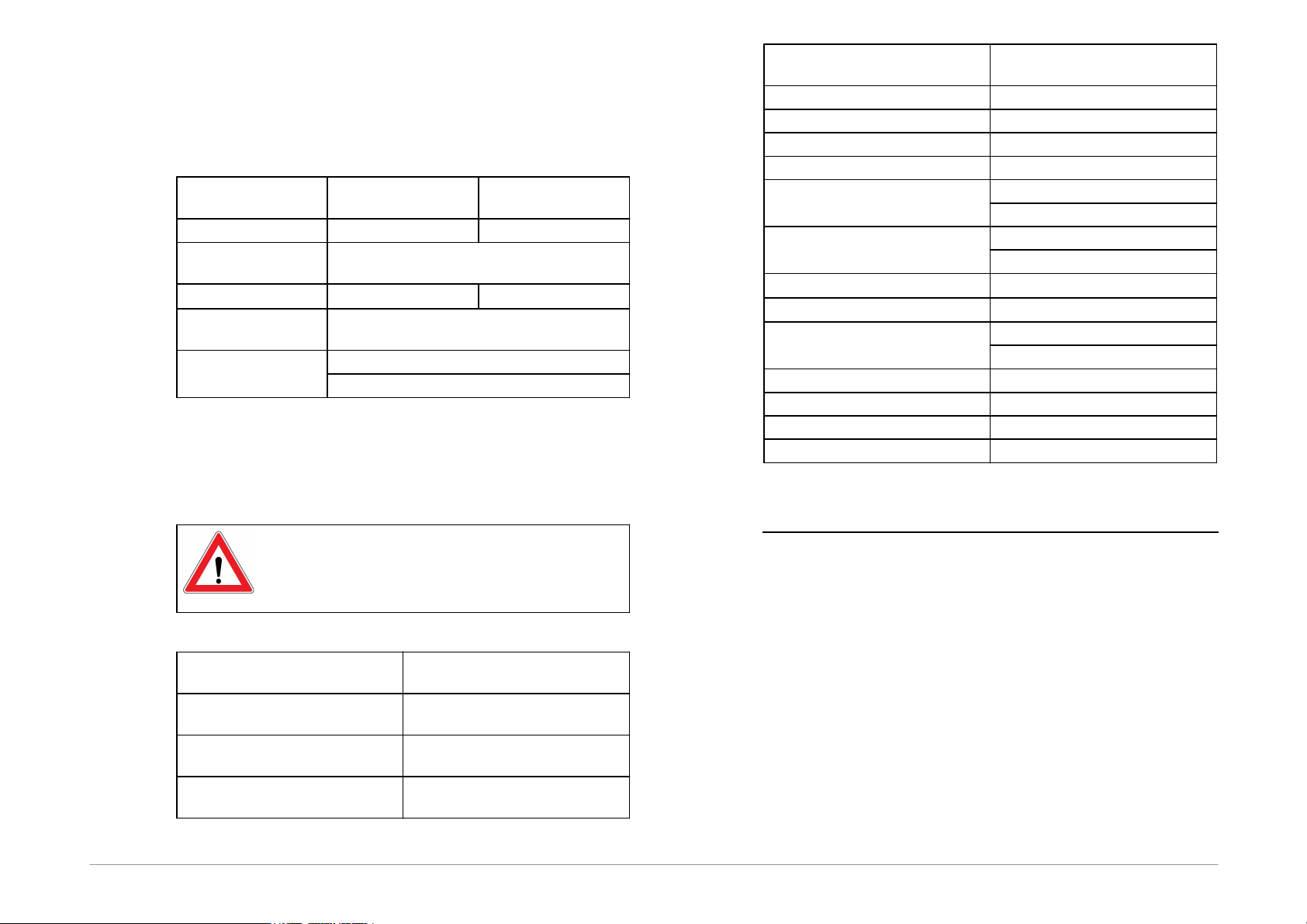
Any voltage peak higher than 7.5V or any current higher
than 20mA on any I/O can cause damage of the
programmer.
Important warning
PRESTO must be connected to a PC and the
UP program must be launched for correct
function of internal protection.
Page 24
2.8
Technical Specifications
2.8.1 Limit Values
Operating
temperature
min. 0°C
max. +55°C
Storage temperature
min. -40°C
max. +85°C
Maximum current on
USB
max. 370mA
Voltage at any pin
1
min. -0.5V
max. 6.5V
Maximum current on
I/O pin
20mA
ESD protection (HBM
model)
±4kV contact
±8kV air
Table7: Limit values
2.8.2 Operating
Specifications
Important Warning
Failure to respect these parameters may
damage the programmer or the connected
computer.
VDD feeding voltage supplied by
programmer
5V
VDD feeding voltage supplied by
application
2.7V to 5.5V
Maximum current drawn from
VDD
100mA
Maximum current drawn from
VPP
50mA
Maximum current drawn from I/
O pin
4mA
Allowed input voltage on pins
0 to 5.5V
P pin output voltage
13V or logic levels
VIL input voltage
max. 0.5V
VIH input voltage
min. 2.0V
VOL output voltage
max. 0.44V @ VDD=4.5V
typ. 0.1V
VOH output voltage
min. 3.8V @ VDD=4.5V
typ. VDD - 0.1V
Resistance to short circuiting
limited
2
Operating system
Windows
3
32/ 64-bit
USB compatibility
USB1.1 Full Speed
USB2.0 compatible
USB connector
type B
Dimensions
112 x 64 x 22mm
Weight
80g
Gross weight
180g
Table8: Operating specifications
1
Pin VPP configured as an output has a voltage +13V
2
For more information see Built-in Protection
3
WindowsXP, WindowsVista, Windows7, Windows8,
Windows8.1, Windows10, Windows11