Utah-94-721002-System-Manual.pdf - 第272页
^ää=lfmq=póëíÉãë l ñÑçêÇ =fåëíê ìãÉåíë =m ä~ëã~=q ÉÅÜåçäçÖó== System Manual RF IN RF OUT DC BIA S COIL C1 COIL C2 C2 P ADDI NG CAP ACITORS C1 P ADDI NG CAP ACITORS TO D C BI AS CIRC UIT TYPICAL MA TCHING COMPONENTS (LA Y…

System Manual lñÑçêÇ=fåëíêìãÉåíë=mä~ëã~=qÉÅÜåçäçÖó== ^ää=lfmq=póëíÉãë
Note that shows an AMU control panel with control facilities for two AMUs. The left-hand
side controls are for AMU1 and the right-hand side controls are for AMU2. The LCD displays
are switched using the DISPLAY SELECTOR switch as shown in the following table.
DISPLAY SELECTOR
POSITION
LCD 1 (UPPER) LCD 2 (LOWER)
1 AMU 1 C1 POSITION AMU 1 C2 POSITION
2 RF 1 FORWARD POWER RF 1 REFLECTED POWER
3 RF 1 SETPOINT RF 1 Hi/Lo
4 RF 2 FORWARD POWER RF 2 REFLECTED POWER
5 RF 2 SETPOINT SPARE
6 AMU 2 C1 POSITION AMU 2 C2 POSITION
For a circuit diagram of the AMU control panel, refer to drawing 94-SE00C23249.
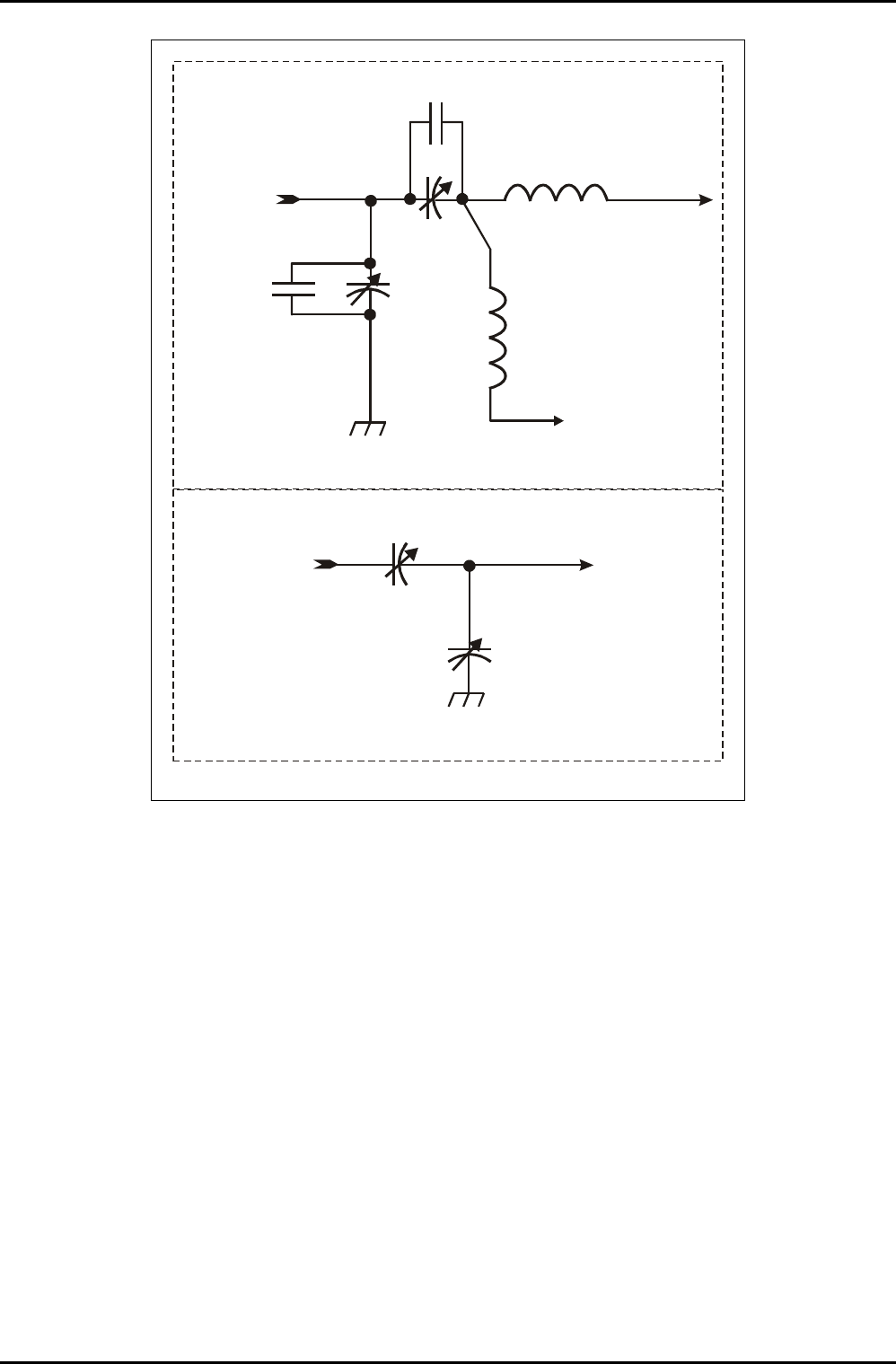
OKP= j~íÅÜáåÖ=ÅçãéçåÉåí=ä~óçìíë=
The layout of the matching components depends on the device to be matched to the RF
Generator to ensure maximum power transfer. Typical layouts of the components are shown
in Fig 3.
Note that in the typical layout, padding capacitors can be added in parallel with C1 and C2 to
modify their capacitance ranges. Refer to sub-section 6.3 (page 19) for details.
OIPT Automatch Unit
Printed: 5-Jan-06, 8:03 Page 5 of 20 Issue 6: February 05
^ää=lfmq=póëíÉãë lñÑçêÇ=fåëíêìãÉåíë=mä~ëã~=qÉÅÜåçäçÖó== System Manual
RF IN
RF OUT
DC BIAS
COIL
C1
COIL
C2
C2 PADDING
CAPACITORS
C1 PADDING
CAPACITORS
TO DC BIAS
CIRCUIT
TYPICAL MATCHING COMPONENTS
(LAYOUT 1)
RF IN RF OUT
C1
C2
ALTERNATIVE MATCHING COMPONENT LAYOUT
(LAYOUT 2)
NOTE: In some systems the circuit labels C1 and C2 are reversed.
Fig 3: Matching component layouts
OIPT Automatch Unit
Issue 6: February 05 Page 6 of 20 Printed: 5-Jan-06, 8:03
System Manual lñÑçêÇ=fåëíêìãÉåíë=mä~ëã~=qÉÅÜåçäçÖó== ^ää=lfmq=póëíÉãë
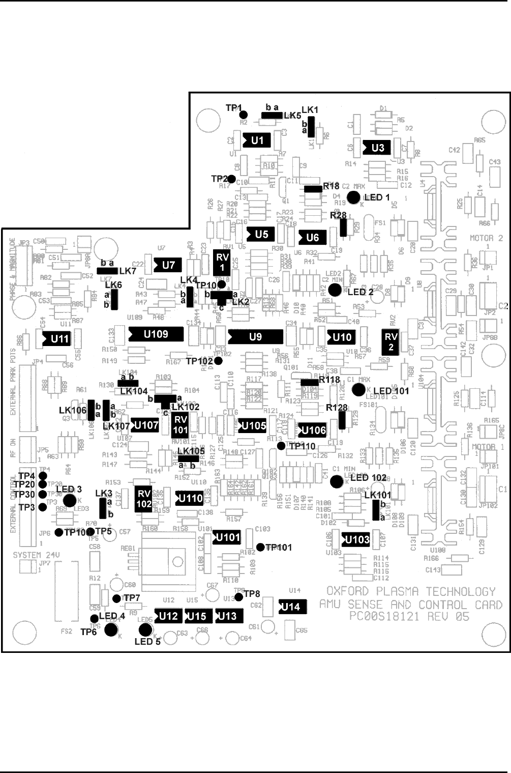
OKQ= pÉåëÉ=~åÇ=Åçåíêçä=m`_=
Refer to drawing 94-SE00A17801 for a circuit diagram of the AMU. The layout of the Sense
and Control PCB is shown in Fig 4 .
Fig 4: Sense and control PCB layout
OIPT Automatch Unit
Printed: 5-Jan-06, 8:03 Page 7 of 20 Issue 6: February 05