PPS Pro version 8.2.pdf - 第54页
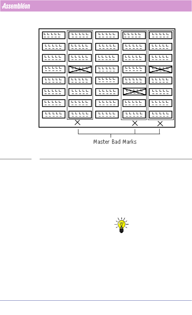
User Manual 4022 591 98247 50 PPS-Pro v8.2 05.07 PPS-Pr o GUI FIGURE 5 Pan el Badm arks The pr ocessing of th e se badmark s takes place as f ollo ws: the camera start s measuring the master badmark s on the PCB . Whene …

4022 591 98247 User Manual
05.07 PPS-Pro v8.2 49
PPS-Pro GUI
Each “bad” board (circuit) contains a circuit badmark (see FIGURE 4 on page
48). Badmarks are detected by a camera.
This camera will perform (in this example) 144 badmark measurements (1 per
circuit) In doing so, the processing time increases the pick-and-place time of
the placement modules. To decrease this influence, the processing time can be
reduced by introducing master badmarks. (And/or area badmarks on A-Series
lines)
Each badmark group has one master badmark. To maintain downward compat-
ibility, the pcb master badmark can also be used.
Two common types of badmarks exist:
1. Panel badmark;
2. Board (circuit) badmark;
In grouping mode multiple panel badmarks can be used. (see 2.19 "Set
Badmark Grouping" on page 56)
For A-Series users it is also possible to specify Area badmarks. (see 2.20 "Area
Badmarks (A-Series)" on page 57)
If more than one badmark type is used and one circuit is bad, the next ‘lower’
level type of badmark has to be provided.
Example: the badmark corresponding to the circuit, the master badmark of
the badmark group (FCM) or Area badmark (A-Series) to which the circuit
belongs, and the PCB master badmark.
For PowerLine users it is important to know that, if all three badmark levels
are available in the PCB description, the generated action specification will
not contain the PCB master badmark, only the circuit badmark and the group
master badmarks will be propagated to the Machine action specification or
Placement Program.
2.16.1 Panel Badmark
A panel badmark corresponds to a group of boards (circuits), each with its
own circuit badmark. If circuit badmarks are also present then panel
badmark(s) will become master badmark(s), they can be interpreted as a
“search” mark indicating that a search for circuit badmarks is necessary
(see
FIGURE 5 on page 50). A panel badmark may appear anywhere on the PCB.
Typically, master badmarks can be placed along a border of the PCB to reduce
travel time between master badmarks.
The figure 5 shows the PCB with 3 panel badmarks indicating a bad circuit in
their respective badmark groups.
User Manual 4022 591 98247
50 PPS-Pro v8.2 05.07
PPS-Pro GUI
FIGURE 5 Panel Badmarks
The processing of these badmarks takes place as follows: the camera starts
measuring the master badmarks on the PCB. Whenever a master badmark is
measured as being ‘bad’, the circuit badmarks of the circuits in the badmark
group will be measured. When a master badmark is not set, then no corre
-
sponding circuit within the badmark group is marked “bad”. Badmark meas-
urement of these circuits can therefore be skipped and time will be saved.
2.17 Fiducal and badmark group editing in the MDF
NOTE: When there are no Badmarks in the MDF-file they have to be added manually
with the MDF editor. Adding is done by Add/Board Reject..., here Board and/
or Panel Badmarks can be created
Fiducial arrangements and badmark groups are not actually tangible entities
that you can see on a board but they are board specific data. This information
is stored within the MDF file. The ‘Group mode’ is provided in which fiducial
arrangements and badmark groups may be created, viewed, deleted, edited
and scrutinized.
4022 591 98247 User Manual
05.07 PPS-Pro v8.2 51
PPS-Pro GUI
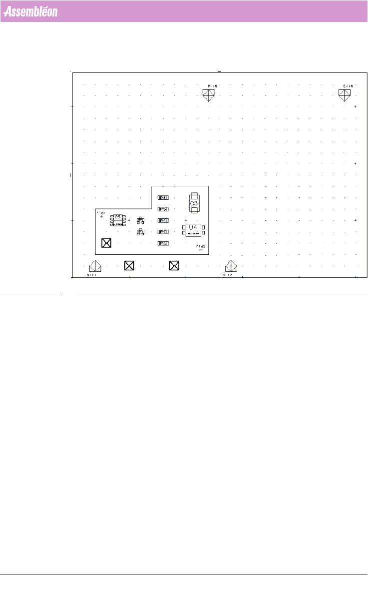
Consider the following panel (see FIGURE 6 on page 51).
FIGURE 6 Panel Starting Point
This panel satisfies the requirements for adding fiducial arrangements and
badmark groups. The board is not flattened and the appropriate step-and-
repeat symbols are present. Fiducials, badmarks, and panel badmarks are also
present.
Only the “base” image is shown but fiducials from any of the four board
instances may be required for selection and inclusion in fiducial
arrangements. It is possible to present the panel in a manner showing all of
the necessary fiducials and badmarks. This actually puts the graphical editor
into a mode that allows only the manipulation of fiducials and badmark
groups. The command File > Group Mode enters that mode
(see FIGURE 7 on
page 52).