SIPLACE CA4 V2规格说明书.pdf - 第31页
31 SIPLACE Wafer System Overview Description The SIPLACE Wafer System (SWS) makes the compo- nents available to the place - ment head, directly from the wafer . The SWS therefore extends the component spectrum of the est…

30
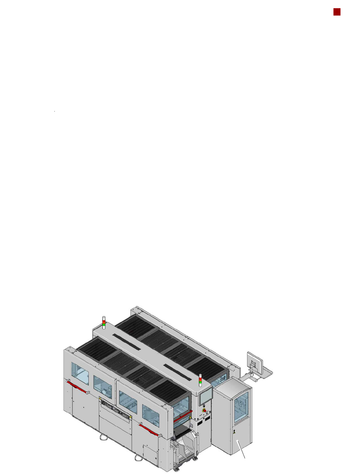
Component feeding
SIPLACE JTF-M
Technical data
SIPLACE JTF-M
Width
177 mm
Height
587 mm
JEDEC waffle pack tray specification
JEDEC Standard: 95-1 & IEC 60286-5
Storage capacity
Waffle pack tray, thin 18 JEDEC waffle pack trays
Thick waffle pack tray 14 JEDEC waffle pack trays
Waffle pack tray changeover time
Slot n to n+1 3.5 seconds
Slot 1 to 18 10 seconds
Slot 18 to 1 8.9 seconds
Cassette
Dimensions approx. 330 mm x 150 mm x 230 mm
Max. load capacity 2.7 kg (150 g each for 18 slots)
Pneumatics
5.2 bar to 9 bar
Compressed air consumption
< 28.3 NL/min.
31
SIPLACE Wafer System
Overview
Description
The SIPLACE Wafer System
(SWS) makes the compo-
nents available to the place-
ment head, directly from the
wafer. The SWS therefore
extends the component
spectrum of the established
SIPLACE X machines, by
enabling placement of bare
dies from wafers.
The wafers are supplied fully
automatically out of the wafer
cassette and the dies inside
can be processed in the
established placement pro-
cedures.
The SWS is completely inte-
grated into the locations of
the SIPLACE CA placement
system. Each location can be
equipped with an SWS or an
X table.
Flip chip process - func-
tion
The wafer is fully automati-
cally pulled out of the wafer
cassette and is then trans-
ported to the wafer table. The
wafer table positions the die
above the ejection system
that releases the die from the
wafer foil. After this release
procedure, the flip unit noz-
zle takes the die, rotates it by
180° and makes it available
to the placement head for
pickup.
Options
The process spectrum is
supplemented by the follow-
ing options:
– Die Attach Unit:
The Die Attach Unit takes
the die from the flip unit
nozzle and turns it, so that
it has the same top-bottom
orientation on the board
as it had on the wafer.
– Linear Dipping Unit
The Linear Dipping Unit
distributes precise layers
of flux for the flip chip pro-
cess. After taking over
from the flip unit, the
placement head dips the
die into the flux layer.
SIPLACE Wafer System (SWS)

32
SIPLACE Wafer System
Component supply
Technical data Flip Chip Die Attach
Minimum die thickness (silicium) - without com-
ponent sensor
50 µm 50 µm
Minimum die thickness (silicium) - with compo-
nent sensor
100 µm 100 µm
Minimum bump size 50 µm n/a
Minimum bump grid 100 µm n/a
SIPLACE Wafer System SWS Horizontal system, automatic wafer change, MCM
SWS wafer size 4" to 12"
4" / 6" with adapter on request
Wafer frame 12“/8“
6" on request
4" with adapter
Wafer frame: Maximum height 12“: 8.1 mm
8": 7.6 mm
6": 5.8 mm
Wafer magazine
a
a) Depending on the wafer magazine, you may need to mechanically adjust the base plate for the wafer magazines.
Up to 12"
Die Ejection System Programmable ejection speed (synchronous and asynchronous)
Option: Linear Dipping Unit LDU Individually programmable speed
Flux viscosity 3,000 to 100,000 cPs
Accuracy of flux height ± 5 µm