SIPLACE CA4 V2规格说明书.pdf - 第6页
6 Machine description Overview General The SIPLACE CA4 V2 (chip assembly) platform can place bare dies directly from the wafer, using the die at- tach or flip chip process. This provides addit ional support for the SMT p…

5
Overview of technical data
Maximum values
Accuracy
a
a) 10µm at 3
σ in placement process with the "Embedded wafer level ballgrid array" option (on request).
Heads
Flip Chip Die Attach SMT
C&P20 M2
CPP M
± 10 µm at 3σ
± 10 µm at 3σ
± 10 µm at 3σ
± 10 µm at 3σ
± 15 µm at 3σ
± 15 µm at 3σ
Placement performance
b
b) The placement performance depends on several project-specific parameters. The ex-
pected throughput can be individually calculated on request.
Heads
Flip Chip Die Attach
4 SWS 4 SWS SMT
C&P20 M2
CPP M
46,000 die/h
41,000 die/h
30,000 die/h
29,000 die/h
126,500 com-
ponents/h
85,500 compo-
nents/h
Die / component size
Heads
Flip Chip Die Attach SMT
C&P20 M2
CPP M
0.5 x 0.5 mm
c
d
to 6 x 6 mm
0.5 x 0.5 mm
c d
to 15 x 15 mm
c) Smaller dies on request
d) Dipping: depends on process
0.8 x 0.8 mm
to 6 x 6 mm
0.8 x 0.8 mm to 15 x 15 mm
See page 10
See page 11
Die / component supply and feeding
Feeder module
types
Tape feeder module, waffle pack tray, stick magazine
feeders, bulk case, dip module, application-specific
OEM feeder modules, SIPLACE Wafer Feeder (SWS)
Supply capacity
(Component trolley
SIPLACE X)
160 tape feeder modules 8 mm X
Component range C&P20 M2: 0.12 mm x 0.12 mm (0201 metric) to 6 mm x 6 mm
CPP M: 0.11 mm x 0.11 mm (01005) to 15 mm x 15 mm
Workpiece carrier -
size
50 mm x 50 mm to 650 mm x 700 mm
Workpiece thick-
ness
0.3
e
mm to 4.5 mm
e) Thinner than 0.3 mm on request

6
Machine description
Overview
General
The SIPLACE CA4 V2 (chip
assembly) platform can
place bare dies directly from
the wafer, using the die at-
tach or flip chip process. This
provides additional support
for the SMT placement op-
tions available with SIPLACE
X-Series S machines. The
SIPLACE CA4 V2 can either
be used only for bare die or
SMT placement or in single
pass mode. In this case, both
bare dies and SMT compo-
nents can be placed during
the same process. Users
benefit from a combination of
greater process flexibility and
higher placement speeds
which is unique to the elec-
tronics production industry.
The SIPLACE CA4 V2 is pro-
vided with 4 gantries and can
be configured with up to 4
SWSs (S
IPLACE Wafer
?S
ystem).
The SWS provides the place-
ment head with components
(dies) directly from the wafer
(max. 12“).
Overview
The SIPLACE CA4 V2 sup-
ports the wafer level fan out
process up to 300 mm diam-
eter with flip chip and die
attach processes, plus the
panel level process with a
maximum workpiece carrier
size of 700 mm x 650 mm.
This machine is therefore the
optimum solution to support
the accuracy and perfor-
mance requirements of the
advanced packaging pro-
cesses. For standard boards
from 50 mm x 50 mm up to
850 mm x 560 mm with long
board option.
The SIPLACE CA4 V2 also
supports virtual inkspot han-
dling (this corresponds to an
electronic substrate map).
The maximum quantity of
placement positions is
120,000 components per
SIPLACE CA4 V2 (200,000
components per panel for
panel level on request).
Placement machine
The placement machine
uses the Collect&Place?
method for high-speed
placement of standard com-
ponents.
The moving head picks the
components up from the
waiting SWS and places
them on the waiting printed
circuit board. This proven
SIPLACE principle has many
advantages:
• No downtime due to refill-
ing or splicing
• Reliable pickup of even
the smallest components
• No shifting of the compo-
nents on the circuit board
• Minimized travel range
High flexibility, economic effi-
ciency and reliable setups
are the guarantee for the
high level of productivity in
theSIPLACE CA4 V2.
Minimum down times
increase utilization and thus
help to increase productivity.
Even the very small 03015/
0201 (metric) components
can be processed with the
SIPLACE CA4 V2.
SIPLACE Wafer System
(SWS)
The integration of the
SIPLACE Wafer Systems
(SWS) in the
SIPLACE CA4 V2 enables
you to place dies directly
from the wafer, using the
standard SMT placement
procedure. This unique
placement platform supports
both the flip chip and the die
attach process.
• Processes supported:
Flip chip, die attach (chip
on board), SMT
• Hoopring handling
• Horizontal wafer system
• Automatic wafer change
• Linear Dipping Unit
• Die attach unit
• Wafer map connection
(e.g. ALPS)
• Multi-die capability
7
Machine description
Overview
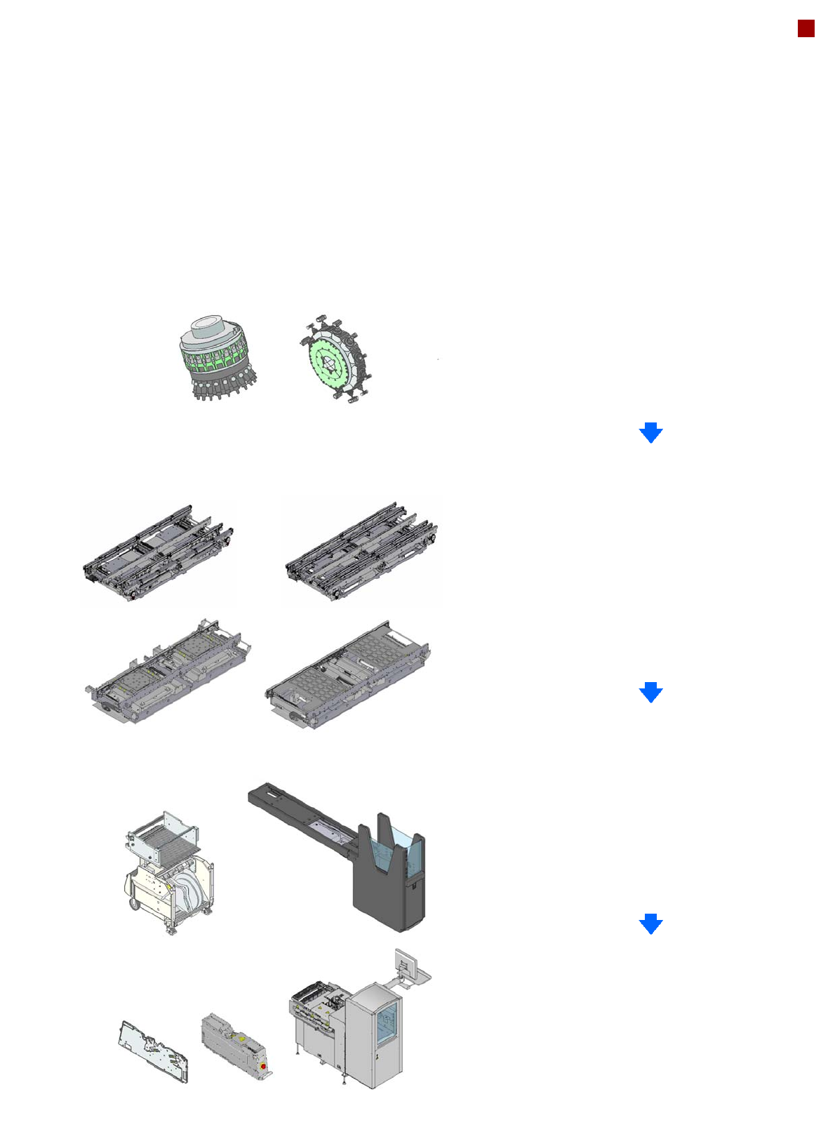
Placement head range available
SpeedStar (C&P20 M)
MultiStar (CPP)
Selection of conveyor
Single lane conveyor
Dual lane conveyor
Panel lane conveyor
Wafer lane conveyor
Selection of component infeed
Component trolley
JTF-M
Feeder modules available
X tape feeder modules
Linear Dipping Unit X
SIPLACE PowerConnector X
SIPLACE Wafer System