SIPLACE CA4 V2规格说明书.pdf - 第35页
35 SIPLACE Vision OnBoard Inspection and Pattern Matching OnBoard Inspection The OnBoard PCB Inspec- tion (SW option) uses the PCB camera to inspect criti- cal areas of the board, spec- ified by the user, e.g. under BGA …

34
SIPLACE Wafer System
List of options
Available options SWS Notes
SIPLACE wafer transfer system (table: 1,3)
X
SIPLACE wafer transfer system (table: 2,4)
X
Adapter FF070 & FF 090 on standard frame FF 108
X
Adapter hoop ring 4" on FF 108
X
Adapter hoop ring 6" on FF 108
X
Adapter hoop ring 8" on FF 108
X
SIPLACE wafer expansion unit for 8" and 12" wafers
X
Wafer holder 8" for standard frame in combination with hoop
ring (table.: 1,3)
X
Wafer holder 8" for standard frame in combination with hoop
ring (table.: 2,4)
X
Wafer holder 12" for standard frame in combination with hoop
ring (table.: 1,3)
X
Wafer holder 12" for standard frame in combination with hoop
ring (table.: 2,4)
X
Wafer holder 8" for standard frame (table: 1,3)
X
Wafer holder 8" for standard frame (table: 2,4)
X
Wafer holder 12" for standard frame (table: 1,3)
X
Wafer holder 12" for standard frame (table: 2,4)
X
Multi needle eject system 3.5 x 3.5 mm min. needle pitch
X
Multi needle eject system 2.0 x 2.0 mm min. needle pitch
X
Small Die Eject System
X
Component handling standard, field of view: 12 mm x 12 mm
X
SIPLACE Linear Dipping Unit (LDU-X)
X
Integrated into the SWS:
Only one LDU per location.
Standard flux pot for LDU-X
X
SIPLACE CA LDU cavity plates, 20 - 400µm in 10µm steps
X
SIPLACE WS die attach unit
X
Nozzle changer C&P 20 M2
X
One bank in row 2
Row 1 on request
Nozzle changer CPP M
X
Single component traceability
X
35
SIPLACE Vision
OnBoard Inspection and Pattern Matching
OnBoard Inspection
The OnBoard PCB Inspec-
tion (SW option) uses the
PCB camera to inspect criti-
cal areas of the board, spec-
ified by the user, e.g. under
BGA or shields just before or
after placement, to make
sure that all components
were placed or to make sure
that there are no objects in
the way of the placement
process.
It is also possible to inspect
the solder paste to make
sure that it is present. How-
ever, this must always be
performed at the first place-
ment machine, before place-
ment begins.
A requirement for all inspec-
tion tasks is that a "good pat-
tern" has been saved before
starting.
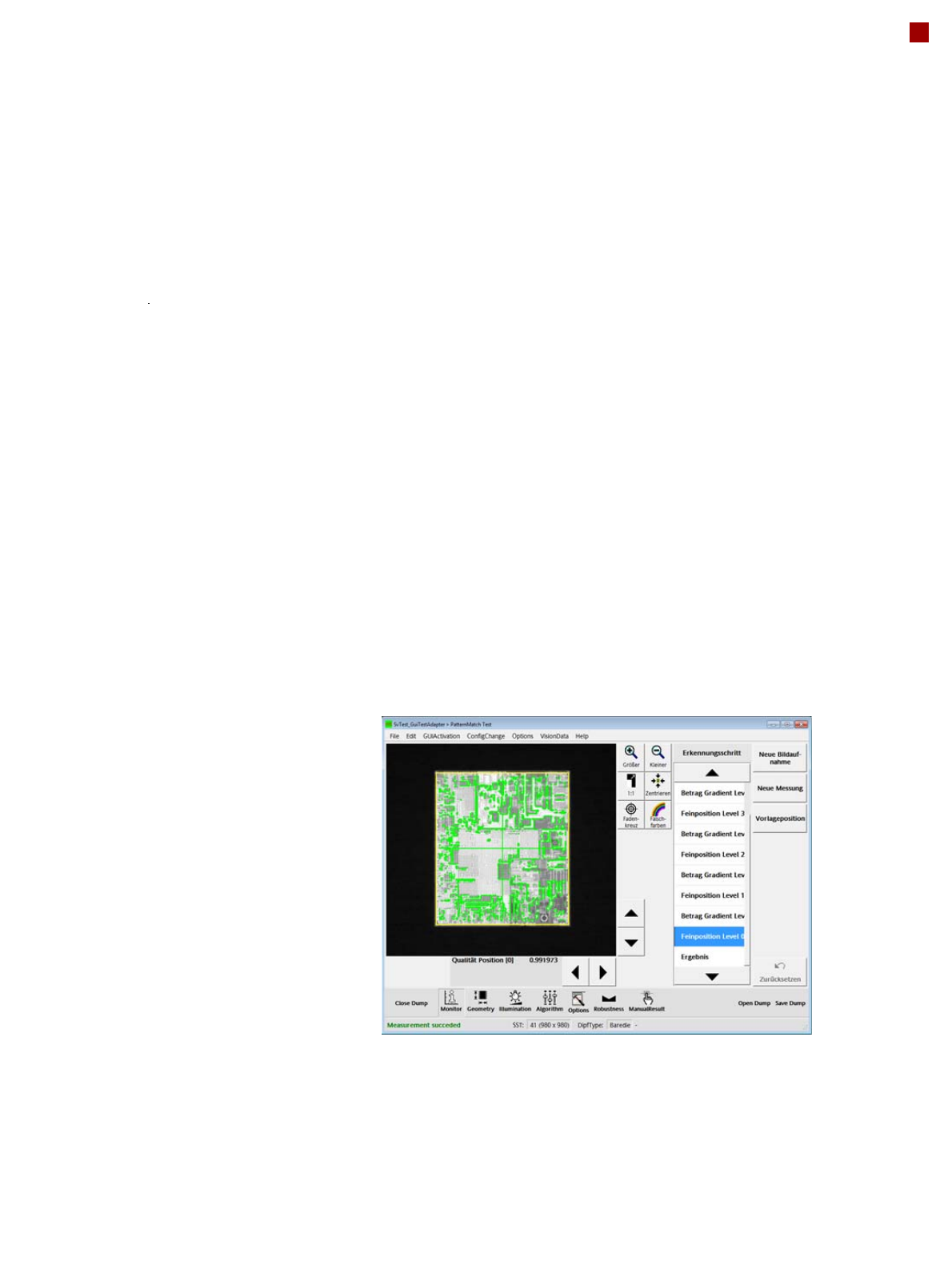
Pattern Matching
Pattern matching can be
used for components with
very fine contact pads, which
can not be detected with the
existing component camera
resolution. Searching and
detection is performed over a
larger area, which contains
unique structures (patterns).
Once the specified area has
been detected, the compo-
nent is aligned and placed
according to the position of
this area and in relation to the
substrate.
36
SIPLACE Vision
Cracked Die and Chipping Detection
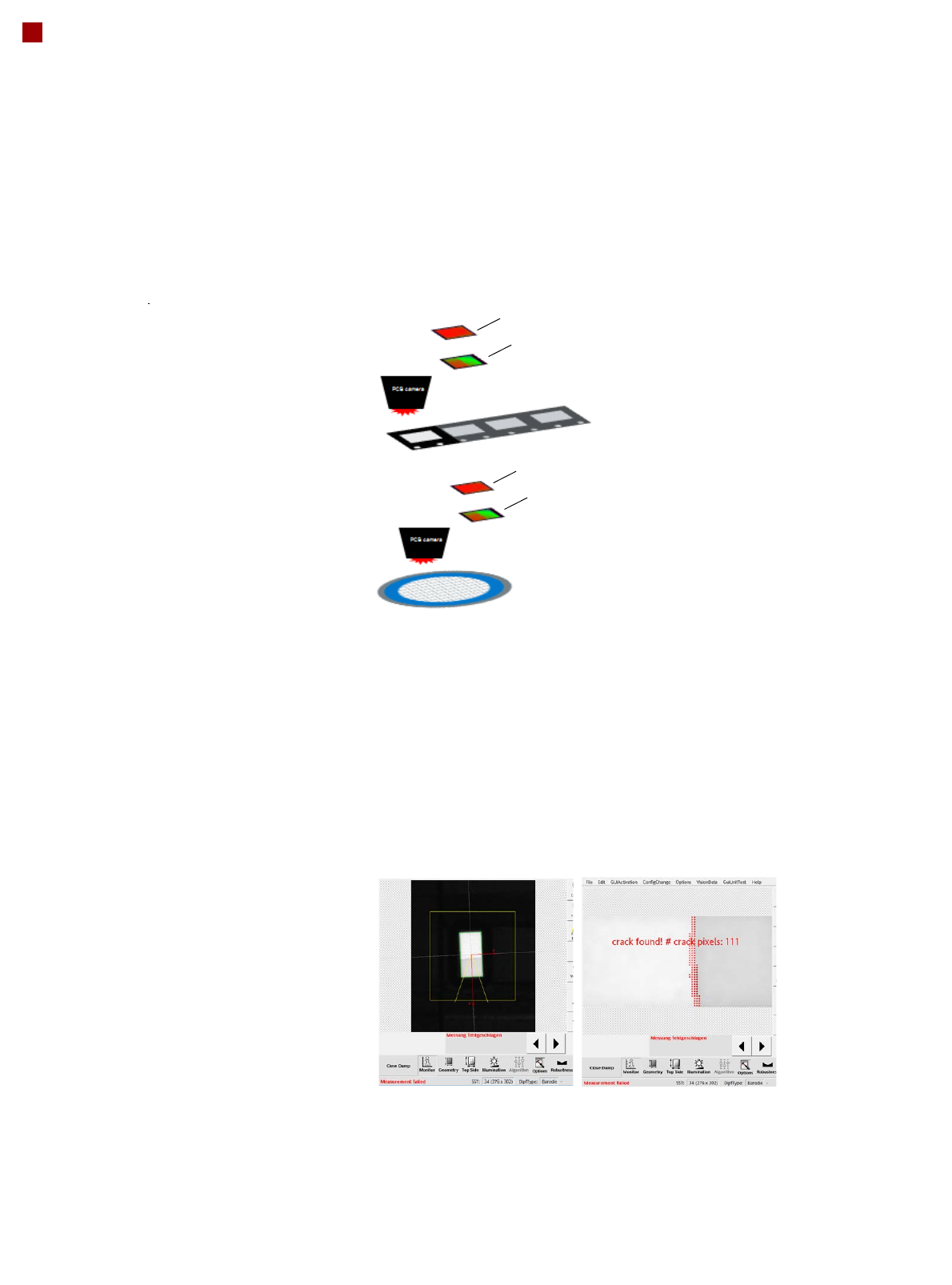
Crack Die Detection
The Cracked Die Detection
can detect breaks before
removal from the tape, if the
crack runs between two
outer edges of the die.
Inspection is performed
with the PCB camera. A
prerequisite for detection is
that the two parts of the die
are slightly inclined towards
one another. Detection is
possible via the differing
reflection angles of the two
surfaces which are inclined
towards one another.
Chipping Inspection
The Chipping Inspection is
used to detect damage
(chips etc.) to semiconductor
parts.
Good
Bad
Good
Bad