SPF维修.pdf - 第125页
SPF 6.6 P783 Jumper Setting List SERVICE MANUAL 6.6−10 D54SEC−85−040−B0 RC F A-M00862-13 2/3 Jumper setting J Functions Connection settings Set- ting J9 Input select to component side flash memory 30 pin 1-2 Connects to …
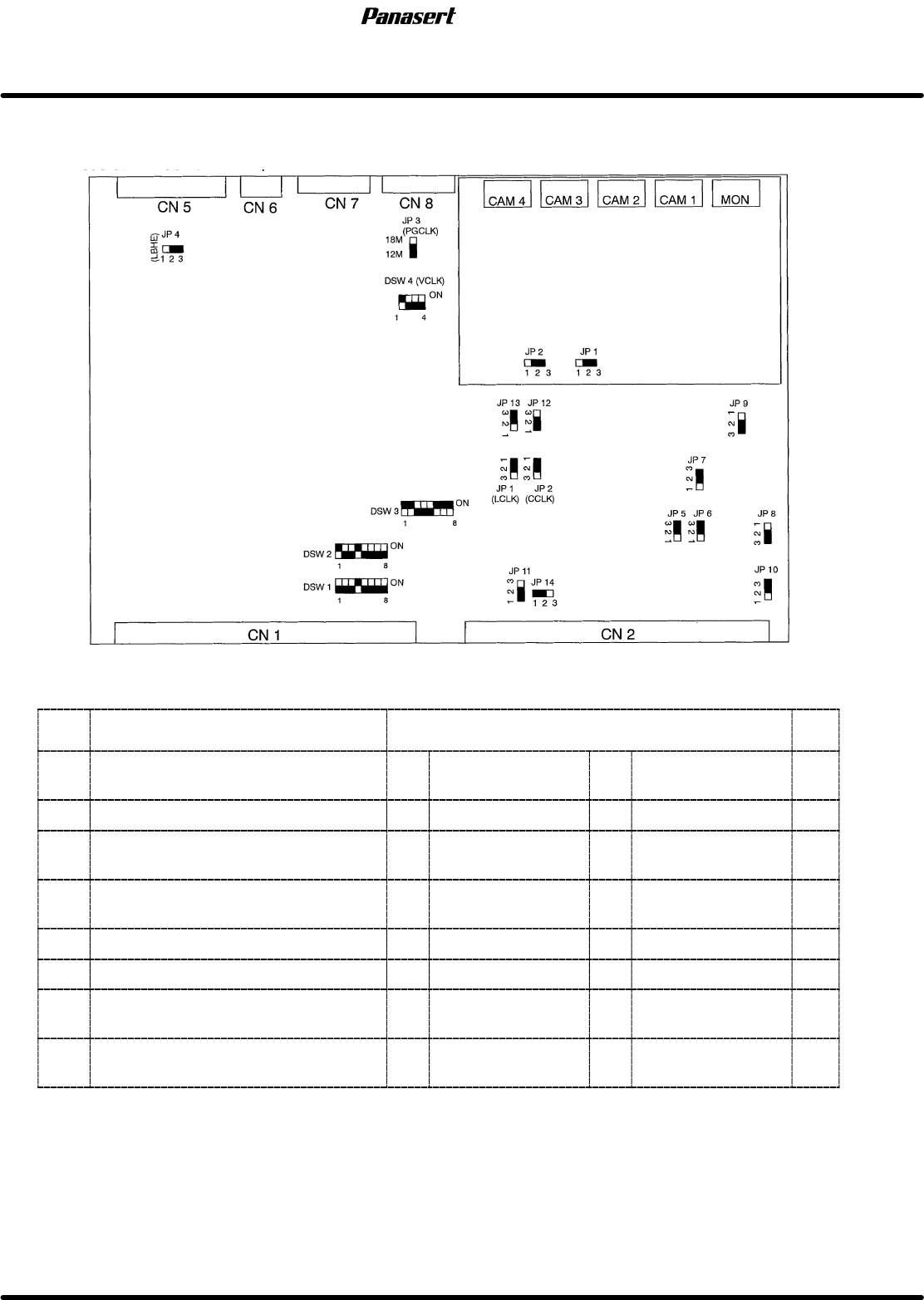
6.6 P783 Jumper Setting List
SERVICE MANUAL
SPF
6.6−9
D54SEC−85−040−B0
RC FA-M00862-13 1/3
Jumper setting
J Functions Connection
Set-
ting
J1
LCLK: Clock output to extended local
bus.
1-2
Connects to GND
2-3
CPU clock
1-2
J2 CCLK: CPU clock frequency select
1-2
40MHz
2-3
20 MHz
1-2
J3
PBCLK: Output clock select to
Piggyback board
1-2
Register setting
2-3
12 MHz
2-3
J4
LBHE: Output select to extended local
bus
1-2
Connects to GND
2-3
Output to BE2
2-3
J5 Flash memory address select
1-2
A21 invalid
2-3
A21 valid
2-3
J6 Flash memory address select
1-2
A20 invalid
2-3
A20 valid
2-3
J7
Component side flash memory address
select
1-2
A21 use
2-3
A19 use
2-3
J8
Input select to component side flash
memory 1 pin
1-2
Connects to A20
2-3
Connects to Vpp
2-3
SPF
6.6 P783 Jumper Setting List
SERVICE MANUAL
6.6−10
D54SEC−85−040−B0
RC FA-M00862-13 2/3
Jumper setting
J Functions Connection settings
Set-
ting
J9
Input select to component side flash
memory 30 pin
1-2
Connects to A19
2-3
Connects to Vcc
2-3
J10
Input select to backside flash memory
9 pin
1-2
Connects to A20
2-3
Connects to Vpp
2-3
J11 Command reset select
1-2
Not reset
2-3
Reset
1-2
J12 Output clock select to P2-CLK0
1-2
18 MHz
2-3
12 MHz
1-2
J13 Output clock select to P2-CLK1
1-2
18 MHz
2-3
12 MHz
2-3
J14
Output voltage select to piggyback
board
1-2
+15V
2-3
+12V
1-2
Dip switch setting
No. Contents Setting
8-MINT 0 OFF
7-MINT 1 OFF
6-MINT 2 OFF
DSW
1
5-MINT 3
Interrupt
signal
OFF
MINT
4
DSW
1
4-MINT 4
Interrupt signal
output
to
P783
ON
MINT
4
3-MINT 5
o
u
tp
u
t
to
P783
bus
OFF
2-MINT 6
bus
ON : 1 OFF
1-MINT 7
OFF : 0
OFF
8-ADR 12 OFF
7-ADR 13 OFF
6-ADR 14 OFF
DSW
2
5-ADR 15
2−port RAM upper
OFF
90000H
DSW
2
4-ADR 16
2 port
RAM
upper
address viewed
f
P
i
ON
90000H
3-ADR 17
from P783 main
board
OFF
2-ADR 18
board
ON : 1
OFF
0
OFF
1-ADR 19
OFF : 0
ON
8−ADR 3 ON
7−ADR 4 ON
6−ADR 5
I/O access address
ON
5−ADR 6
/O
access
add ess
viewed from P783 main
board
OFF
238H
DSW 3
4−ADR 7
board
OFF
3−ADR 8
ON : 1
OFF
0
OFF
2−ADR 9
OFF : 0
ON
1 −−−−−
I/O access mode select
ON : P872 mode OFF : P880 mode
ON P872 mode
6.6 P783 Jumper Setting List
SERVICE MANUAL
SPF
6.6−11
D54SEC−85−040−B0
RC FA-M00862-13 3/3
Dip switch setting
No. Contents Setting
1 −−−−−
Selection of clock inputted from CN2 (bus)
ON : Image clock 1 (B44 PIN)
OFF : Image clock 2 (A19 PIN)
ON Image clock 1
2−−−−− Not used OFF
DSW 4
3−−−−−
Connection of clock to CN2 (bus)
ON : Output 18MHz to P2 image clock 1
OFF : Not output
OFF Not output
4−−−−−
Connection of clock to CN2 (bus)
ON : Output 12MHz to P2 image clock 2
OFF : Not output
OFF Not output